Download
1 / 17
210 likes | 509 Views
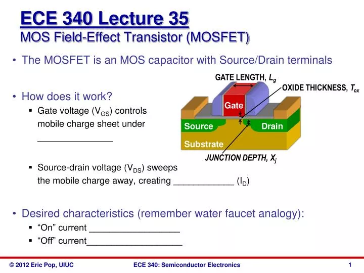
ECE 340 Lecture 35 MOS Field-Effect Transistor (MOSFET). The MOSFET is an MOS capacitor with Source/Drain terminals How does it work? Gate voltage (V GS ) controls mobile charge sheet under _______________ Source-drain voltage (V DS ) sweeps

E N D
ECE 340 Lecture 35MOS Field-Effect Transistor (MOSFET) • The MOSFET is an MOS capacitor with Source/Drain terminals • How does it work? • Gate voltage (VGS) controls mobile charge sheet under _______________ • Source-drain voltage (VDS) sweeps the mobile charge away, creating ____________ (ID) • Desired characteristics (remember water faucet analogy): • “On” current __________________ • “Off” current___________________
First MOSFET patents: Julius Lilienfeld (early 1930s) • This invalidated most of Bardeen, Brattain and Shockley’s transistor patent claims in the late 1940s! • But the MOSFET did not work in practice until the 1960s. Why?
A modern “n-type” MOSFET (N-MOSFET): • How does it work? • If VG = 0, any current between source-drain (ID)? • If VG > 0 what happens (assume source grounded, VS = 0) • If VGS >> 0 and VDS > 0 what happens?
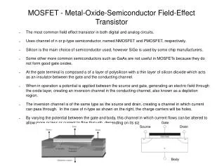
Typical 2-D cross-section view of the N-MOSFET: • Note direction of carrier flow, and of current flow • Gate voltage (VGS) controls Source-to-Drain current (ID) • “Source” terminal refers to source of _____________ ID ID VGS VGS
Theory of the MOSFET (*here N-MOSFET): • When VGS < VT the channel is _________________ • When VGS > VT the channel is _________________ • If small drain voltage (VDS > 0) is applied __________ • Will charge sheet move by drift or diffusion? Current ≈ width X charge sheet X velocity • What is the inversion charge: |Qinv| ≈ • What is the drift velocity: v ≈
At low VDS, the inversion layer essentially acts like a resistor! • What about higher drain voltages VDS? • Must take into account variation of potential along channel, 0 < Vx < VDS. So inversion layer charge at any point is |Qinv(x)| = Ci(VGS – VT – Vx) • And the current is: IDS,lin = • Still linear in VGS voltage! This is the linear region. • When VDS = VGS – VT the channel becomes _____________
When VDS > VGS - VT the un-inverted (drain depletion) region increases, as does the ____________________ • Any increase in VDS: • Reduces the amount of inversion charge, but… • Increases the lateral field (charge velocity) • The two effects cancel each other out, so at high VDS the drain current is no longer a function of VDS! The current saturates to a value only dependent on VGS (i.e. charge). • Putting in VDS = VGS – VT (the pinch-off, i.e. saturation condition) in the previous equation:
Plot and label an example N-MOSFET: • What about IDS vs. VGS? Z dox VT
Back to the physical picture, why does ID vs. VDS saturate? • Why is this desirable? • Voltage gain, dVDS/dID because small changes in ID cause large swings in VDS
What is the “effective mobility” μeff in the MOSFET channel? • Can we look it up in the bulk-silicon charts? • Scattering mechanisms affecting mobility in channel: • Charged impurity (Coulomb) scattering • Lattice vibration (phonon) scattering • Surface roughness scattering
ECE 340 Lecture 36MOSFET Analog Amplifier and Digital Inverter • Analog applications: Small-Signal MOSFET model • Of all elements in the model… CGS ~ Ci and gm (transconductance dID/dVGS) are essential, the rest are parasitics which must be reduced • Note that a lot of elements are voltage-dependent, e.g. depletion capacitances vary with depletion widths and voltage
Drain current: • Conductance parameters: • See ECE 342, ECE 441 At low frequency At high frequency output conductance transconductance
Cutoff frequency fmax = frequency where MOSFET no longer amplifies input (gate) signal • Obtained by considering high-freq. small-signal model with output shorted, finding freq. where |iout/iin| = 1 • Something we already knew qualitatively higher MOSFET operating frequency achieved by decreasing channel length L, increasing mobility μeff • Smaller = faster for devices (though parasitics play a big role in realistic circuits)
Logic applications: CMOS inverter • Key property: signal regeneration – returns logic outputs (0 or 1=V+=VDD) even in presence of noise • Complementary MOS (CMOS) inverter
Qualitative operation: • When Vin = 0 Vout = NFET is ________ PFET is __________ • When Vin = VDD Vout = NFET is ________ PFET is __________ • Other key property of CMOS inverter: no power consumption while idling in either logic state (only while switching) • Consider PFET as “load” to NFET: • Note “rail-to-rail” logic levels 0 and VDD • Want transition voltage VDD/2, but usually Lp = Ln which means choose Zp/Zn ≈ 2 because μn ≈ 2μp (for Si)* *what about other materials?
A quick look at CMOS power dissipation • Energy consumed while charging capacitive load: EP = _______ • CL is discharged through NFET EN = _________ • Total energy dissipated per clock cycle: E = CLVDD2 • Frequency f cycles per second active power P = fCLVDD2 • This is very important: fundamental trade-off between speed (f) and power dissipation. Reducing voltage and parasitic C’s is a must to keep power low at higher speeds.
In reality, there is also passive power (leakage) dissipated by the FETs supposed to be “off”: Poff = IleakVDD • Ioff ~ Ion/1000 in modern technology per transistor • But this can become a headache when you have 100s of millions of “sleeping” transistors (i.e. “passive power” vs. “active power”)! Ex: see IBM journal of Research & Dev. http://www.research.ibm.com/journal/rd/504/tocpdf.html