Download
1 / 96
1.36k likes | 1.95k Views
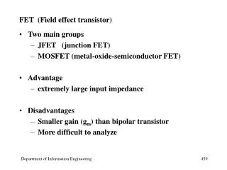
Field Effect Transistor (FET). Basher Yousef Mohsen ( assist. Lecturer bashermohson@yahoo.com. Outlines. Introduction to Field Effect Transistors (FET). JFET Parameters. Biasing JFETs. Metal Oxide Semiconductor Field Effect Transistors (MOSFET). Biasing MOSFET.

E N D
Field Effect Transistor (FET) Basher Yousef Mohsen ( assist. Lecturer bashermohson@yahoo.com
Outlines • Introduction to Field Effect Transistors (FET) • JFET Parameters • Biasing JFETs • Metal Oxide Semiconductor Field Effect Transistors (MOSFET) • Biasing MOSFET Basher Yousef Mohsen ( assist. Lecturer bashermohson@yahoo.com
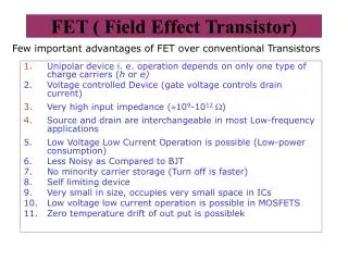
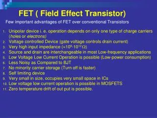
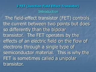
FET - Introduction BJTs (bipolar junction transistors) were covered in previous chapters. Now we will discuss the second major type of transistor, the FET (field-effect transistor). Recall that a BJT is a current-controlled device; that is, the base current controls the amount of collector current. A FET is different. It is a voltage-controlled device, where the voltage between two of the terminal (gate and source) controls the current through the device. The FET’s major advantage over the BJT is high input resistance. Overall the purpose of the FET is the same as the BJT. Basher Yousef Mohsen ( assist. Lecturer bashermohson@yahoo.com
The JFET The junction field effect transistor, like a BJT, controls current flow. The difference is the way this is accomplished. The JFET uses voltage to control the current flow. As you will recall the transistor uses current flow through the base-emitter junction to control current. JFETs can be used as an amplifier just like the BJT. Basher Yousef Mohsen ( assist. Lecturer bashermohson@yahoo.com
The JFET Figure (a) shows the basic structure of an n-channel JFET (junction field-effect transistor). Wire leads are connected to each end of n-channel; the drain is at the upper end, and the source is at the lower end. Two p-type regions are diffused in the n-channel, and both p-type regions are connected to the gate lead. Basher Yousef Mohsen ( assist. Lecturer bashermohson@yahoo.com
The JFET – Basic Operation Figureshows dc bias voltages applied to an channel device. VDD provides a drain-to-source voltage and supplies current from drain to source. The current is controlled by a field that is developed by the reverse biased gate-source junction (gate is connected to both sides). With more VGG (reverse bias) the field (in white) grows larger. This field or resistance limits the amount of current flow through RD. The JFET is always operated with the gate-source pn junction reverse-biased. Basher Yousef Mohsen ( assist. Lecturer bashermohson@yahoo.com
The JFET – Basic Operation Effects of VGS on channel width, resistance, and drain current (VGG = VGS). Basher Yousef Mohsen ( assist. Lecturer bashermohson@yahoo.com
JFET Characteristics and Parameters Let’s first take a look at the effects with a VGS = 0V. ID increases proportionally with increases of VDD (VDSincreases as VDD is increased). This is called the ohmic region (point A to B) because VDS and ID are related by Ohm’s law. As VDS increases from point B to point C, the reverse-bias voltage from gate to drain (VGD) produces a depletion region large enough to offset the increase in VDS, thus keeping ID relatively constant. The drain characteristic curve of a JFET for VGS = 0 showing pinch-off. Basher Yousef Mohsen ( assist. Lecturer bashermohson@yahoo.com
JFET Characteristics and Parameters – Pinch-Off Voltage The point when ID ceases to increase regardless of VDD increases is called the pinch-off voltage (point B). This current is called maximum drain current (IDSS). Breakdown (point C) is reached when too much voltage is applied. This of course undesirable, so JFETs operation is always well below this value. Because breakdown can result in irreversible damage to the device. Basher Yousef Mohsen ( assist. Lecturer bashermohson@yahoo.com
JFET action that produces the characteristic curve for VGS = 0 V.
JFET Characteristics and Parameters – VGS Controls ID From this set of curves you can see with increased voltage applied to the gate the ID is limited and of course the pinch-off voltage is lowered as well. Notice that ID decreases as the magnitude of VGS is increased to larger negative values because of the narrowing of the channel. Pinch-off occurs at a lower VDS as VGS is increased to more negative values. Basher Yousef Mohsen ( assist. Lecturer bashermohson@yahoo.com
JFET Characteristics and Parameters – VGS Controls ID Basher Yousef Mohsen ( assist. Lecturer bashermohson@yahoo.com
JFET Characteristics and Parameters – Cutoff Voltage We know that as VGSis increased IDwill decrease. The value of VGS that makes ID approximately zero is the cutoff voltage (VGS(off)). The field (in white) grows such that it allows practically no current to flow through. The JFET must be operated between VGS = 0 and VGS(off). It is interesting to note that pinch-off voltage (VP) and cutoff voltage (VGS(off)) are both the same value only opposite polarity. Basher Yousef Mohsen ( assist. Lecturer bashermohson@yahoo.com
Comparison of Pinch-Off and Cutoff As you have seen, there is a difference between pinch-off and cutoff. There is also a connection. VP is the value of VDS at which the drain current becomes constant and is always measured at VGS = 0 V. However, pinch-off occurs for VDS values less than VP when VGS is nonzero. So, although VP is a constant, the minimum value of VDS at which ID becomes constant varies with VGS. VGS(off) andVP are always equal in magnitude but opposite in sign. Basher Yousef Mohsen ( assist. Lecturer bashermohson@yahoo.com
Ex. 7-1For the JFET in Figure, VGS(off) = - 4 V and IDSS = 12 mA. Determine the minimum value of VDD required to put the device in the constant-current area of operation. Since VGS(off) = - 4 V, VP = 4 V. The minimum value of VDS for the JFET to be in its constant-current area is VDS = VP = 4 V In the constant-current area with VGS = 0 V, ID = IDSS = 12 mA The drop across the drain resistor is VRD = IDRD = (12 mA)(560Ω) = 6.72 V Apply Kirchhoff’s law around the drain circuit. VDD = VDS + VRD = 4 V + 6.72 V = 10.7 V Ω This is the value of VDD to make VDS = VP and put the device in the constant-current area. Basher Yousef Mohsen ( assist. Lecturer) bashermohson@yahoo.com
JFET Characteristics and Parameters –JFET Transfer Characteristic Curve The transfer characteristic curve illustrates the control VGShas on IDfrom cutoff (VGS(off) ) to pinch-off (VP). A JFET transfer characteristic curve is nearly parabolic in shape and can be expressed as JFET transfer characteristic curve (n-channel). Example of the development of an n-channel JFET transfer characteristic curve (blue) from the JFET drain characteristic curves (green).
Ex. 7-2 A particular p-channel JFET has a VGS(off) = + 4 V. What is ID when VGS = + 6 V? Ans. ID remains 0. Ex. 7-3 The data sheet for a 2N5459 JFET indicates that typically IDSS = 9 mA and VGS(off) = - 8 V (maximum). Using these values, determine the drain current for VGS = 0 V, -1 V, and – 4 V. For VGS = 0 V, ID = IDSS = 9 mA For VGS = - 1 V, For VGS = - 4 V, Basher Yousef Mohsen ( assist. Lecturer bashermohson@yahoo.com
JFET Biasing Just as we learned that the bi-polar junction transistor must be biased for proper operation, the JFET too must be biased for operation. Let’s look at some of the methods for biasing JFETs. In most cases the ideal Q-point will be the middle of the transfer characteristic curve which is about half of the IDSS. The purpose of biasing is to select the proper dc gate-to-source voltage to establish a desired value of drain current and, thus, a proper Q-point. Basher Yousef Mohsen ( assist. Lecturer bashermohson@yahoo.com
JFET Biasing – Self-Bias Self-bias is the most common type of biasing method for JFETs. Notice there is no voltage applied to the gate. The voltage to ground from here will always be VG = 0V. However, the voltage from gate to source (VGS) will be negative for n channel and positive for p channel keeping the junction reverse biased. This voltage can be determined by the formulas below. ID= ISfor all JFET circuits. (n channel) VGS = VG – VS = -IDRS (p channel) VGS = +IDRS VD = VDD – IDRD VDS = VD – VS = VDD – ID(RD + RS) where VS = IDRS
Ex. 7-4 Find VDS and VGS in Figure. For the particular JFET in this circuit, the internal parameter values such as gm, VGS(off), and IDSS are such that a drain current (ID) of approximately 5 mA is produced. Another JFET, even of the same type, may not produce the same results when connected in this circuit due the variations in parameter values. VS = IDRS = (5 mA)(68Ω) = 0.34 V VD = VDD – IDRD = 15 V – (5 mA)(1.0kΩ) = 15 V – 5 V = 10 V Ω Therefore, VDS = VD – VS = 10 V – 0.34 V = 9.66 V Since VG = 0 V, VGS = VG – VS = 0 V – 0.34 V = – 0.34V Basher Yousef Mohsen ( assist. Lecturer bashermohson@yahoo.com
JFET Biasing – Setting the Q-point of a Self-Biased JFET Setting the Q-point requires us to determine a value of RS that will give us the desired ID and VGS.. The formula below shows the relationship. RS= | VGS/ID | To be able to do that we must first determine the VGS and IDfrom the either the transfer characteristic curve or more practically from the formula below. The data sheet provides the IDSSand VGS(off). VGSis the desired voltage to set the bias. ID= IDSS(1 - VGS/VGS(off))2 Basher Yousef Mohsen ( assist. Lecturer bashermohson@yahoo.com
Ex. 7-5 Determine the value of RS required to self-bias an n-channel JFET that has the transfer characteristic curve shown in Figure at VGS = - 5 V. From the graph, ID = 6.25 mA when VGS = - 5 V. Calculate RS. Basher Yousef Mohsen ( assist. Lecturer bashermohson@yahoo.com
Ex. 7-6 Determine the value of RS required to self-bias an p-channel JFET with IDSS = 25 mA and VGS(off) = 15 V. VGS is to be 5 V. Now, determine RS. Basher Yousef Mohsen ( assist. Lecturer bashermohson@yahoo.com
JFET Biasing – Voltage-Divider Bias Voltage-divider bias can also be used to bias a JFET. R1and R2are used to keep the gate-source junction in reverse bias. Operation is no different from self-bias. Determining ID, VGS for a JFET voltage-divider circuit with VD given can be calculated with the formulas below. : Source voltage : Gate voltage : Gate-to-source voltage : Drain current Basher Yousef Mohsen ( assist. Lecturer bashermohson@yahoo.com
Ex. 7-7 Determine ID and VGS for the JFET with voltage-divider bias in Figure, given that for this particular JFET the internal parameter values are such that VD≈ 7 V. Ω Ω Calculate the gate-to-source voltage as follows: Ω Ω Basher Yousef Mohsen ( assist. Lecturer bashermohson@yahoo.com
Representation of the basic E-MOSFET construction and operation (n-channel). Representation of the basic structure of D-MOSFETs. The MOSFET The metal oxide semiconductor field effect transistor (MOSFET) is the second category of FETs. The chief difference is that there no actual pn junction as the p and n materials are insulated from each other. MOSFETs are static sensitive devices and must be handled by appropriate means. There are depletion MOSFETs (D-MOSFET) and enhancement MOSFETs (E-MOSFET). Note the difference in construction. The E-MOSFET has no structural channel.
The MOSFET – Depletion MOSFET The D-MOSFET can be operated in either of two modes – the depletion mode or enhancement mode – and is sometimes called a depletion/enhancement MOSFET. Since the gate is insulated from the channel, either positive or a negative gate voltage can be applied. The n-channel MOSFET operates in the depletion mode when a negative gate-to-source voltage is applied and in the enhancement mode when a positive gate-to-source voltage is applied. These devices are generally operated in the depletion mode. Basher Yousef Mohsen ( assist. Lecturer bashermohson@yahoo.com
The MOSFET – Depletion MOSFET Depletion Mode With a negative gate voltage, the negative charges on the gate repel conduction electrons from the channel, leaving positive ions in their place. Thereby, the n channel is depleted of some of its electrons, thus decreasing the channel conductivity. The greater the negative voltage on the gate, the greater the depletion of n-channel electrons. At sufficiently negative gate-to-source voltage, VGS(off), the channel is totally depleted and drain current is zero. Enhancement Mode With a positive gate voltage, more conduction electrons are attracted into the channel, thus increasing (enhancing) the channel conductivity. Source D-MOSFET schematic symbols. Basher Yousef Mohsen ( assist. Lecturer bashermohson@yahoo.com
The MOSFET – Enhancement MOSFET (E-MOSFET) The E-MOSFET operates only in the enhancement mode and has no depletion mode. It differs in construction from the D-MOSFET in that it has no structural channel. Notice in Figure (a) that the substrate extends completely to the SiO2 layer. For n-channel device, a positive gate voltage above threshold value induces a channel by creating a thin layer of negative charges in the substrate region adjacent to the SiO2 layer, as shown in Figure (b). Representation of the basic E-MOSFET construction and operation (n-channel).
The MOSFET – Enhancement MOSFET (E-MOSFET) The schematic symbols for the n-channel and p-channel E-MOSFET are shown in Figure below. The conventional enhancement MOSFETs have a long thin lateral channel as shown in structural view in Figure below. n Source Basher Yousef Mohsen ( assist. Lecturer bashermohson@yahoo.com
MOSFET Characteristics and Parameters –D-MOSFET Transfer Characteristic As previously discussed, the D-MOSFET can operate with either positive or negative gate voltages. This is indicated on the general transfer characteristic curves in Figure for both n-channel and p-channel MOSFETs. The point on the curves where VGS = 0 corresponds to IDSS. The point where ID = 0 corresponds to VGS(off). As with the JFET, VGS(off) = -VP. D-MOSFET general transfer characteristic curves. Basher Yousef Mohsen ( assist. Lecturer bashermohson@yahoo.com
Ex. 7-8 For a certain D-MOSFET, IDSS = 10 mA and VGS(off) = - 8 V. (a) Is this an n-channel or a p-channel? (b) Calculate ID at VGS = - 3 V (c) Calculate ID at VGS = + 3 V. • The device has a negative VGS(off); • therefore, it is a n-channel MOSFET. Basher Yousef Mohsen ( assist. Lecturer bashermohson@yahoo.com
MOSFET Characteristics and Parameters –E-MOSFET Transfer Characteristic The E-MOSFET for all practical purposes does not conduct until VGS reaches the threshold voltage (VGS(th)). ID when it is when conducting can be determined by the formulas below. The constant K must first be determined. ID(on)is a data sheet given value. K = ID(on) /(VGS - VGS(th))2 ID= K(VGS - VGS(th))2 An n-channel device requires a positive gate-to-source voltage, and a p-channel device requires a negative gate-to-source voltage. E-MOSFET general transfer characteristic curves.
First, solve for K using Equation, Next, using the value of K, calculate ID for VGS = 5 V. Ex. 7-9 The data sheet for a 2N7008 E-MOSFET gives ID(o n)= 500 mA (minimum) at VGS = 10 V and VGS(th) = 1 V. Determine the drain current for VGS = 5 V. Basher Yousef Mohsen ( assist. Lecturer bashermohson@yahoo.com
MOSFET Biasing – D-MOSFET Bias The three ways to bias a MOSFET are zero-bias, voltage-divider bias, and drain-feedback bias. For D-MOSFET zero biasing as the name implies has no applied bias voltage to the gate. The input voltage swings it into depletion and enhancement mode. Since VGS = 0, ID = IDSS as indicated. VDS = VDD - IDSSRD
Since ID = IDSS = 12 mA, the drain-to-source voltage is VDS = VDD – IDSSRD = 18 V – (12 mA)(560Ω) = 11.28 V Ex. 7-10 Determine the drain-to-source voltage in the circuit of Figure. The MOSFET data sheet gives VGS(off) = - 8 V and IDSS = 12 mA. 560 Ω MΩ Basher Yousef Mohsen ( assist. Lecturer bashermohson@yahoo.com
Basher Yousef Mohsen ( assist. Lecturer bashermohson@yahoo.com
Basher Yousef Mohsen ( assist. Lecturer bashermohson@yahoo.com
Basher Yousef Mohsen ( assist. Lecturer bashermohson@yahoo.com
Basher Yousef Mohsen ( assist. Lecturer bashermohson@yahoo.com
Basher Yousef Mohsen ( assist. Lecturer bashermohson@yahoo.com
Basher Yousef Mohsen ( assist. Lecturer bashermohson@yahoo.com
Basher Yousef Mohsen ( assist. Lecturer bashermohson@yahoo.com
Basher Yousef Mohsen ( assist. Lecturer bashermohson@yahoo.com
Basher Yousef Mohsen ( assist. Lecturer bashermohson@yahoo.com
Basher Yousef Mohsen ( assist. Lecturer bashermohson@yahoo.com
Basher Yousef Mohsen ( assist. Lecturer bashermohson@yahoo.com
Basher Yousef Mohsen ( assist. Lecturer bashermohson@yahoo.com
Basher Yousef Mohsen ( assist. Lecturer bashermohson@yahoo.com
Basher Yousef Mohsen ( assist. Lecturer bashermohson@yahoo.com