Download
1 / 61
610 likes | 619 Views
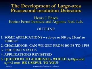
The Development of Large-area Picosecond-resolution Detectors. Henry J. Frisch Enrico Fermi Institute and Argonne Natl. Lab. OUTLINE. SOME APPLICATIONS – sub-ps to 100 ps; 25cm 2 to 10,000 m 2 GRAND CHALLENGE: Can we get from 100 ps to 1 ps? If not, why not? (if so, 0.1 ps?? Limit?)

E N D
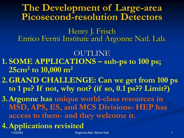
The Development of Large-area Picosecond-resolution Detectors Henry J. Frisch Enrico Fermi Institute and Argonne Natl. Lab. OUTLINE • SOME APPLICATIONS – sub-ps to 100 ps; 25cm2 to 10,000 m2 • GRAND CHALLENGE: Can we get from 100 ps to 1 ps? If not, why not? (if so, 0.1 ps?? Limit?) • Argonne has unique world-class resources in MSD, APS, ES, and MCS Divisions- HEP has access to them- and they welcome it. • Applications revisited Argonne Alan Stone Visit
Fast Timing and TOF in HEP Henry Frisch Enrico Fermi Institute, University of Chicago Long-standing motivation- understanding the basic forces and particles of nature- hopefully reflecting underlying symmetries CDF-1979 to present Discoveries: Top quark B_s Mixing Measurements: Many many many- and many more not done yet Not light compared to Atlas and CMS ( 5000 tons) Argonne Alan Stone Visit
Fast Timing and TOF in HEP • I believe that the existence of ‘flavor’- up, down, strange, charm, bottom, and top is essential, in the sense that if we can’t understand it in a deeper way, we’re in the grip of initial conditions rather than fundamental symmetries or principles. • Really a deep divide between the string landscape community, who are stuck with 10500 equally possible universes, and us, who have this one characterized by small integers and interesting patterns. (Aside- This latter, I believe, is the future area for Fermilab). Argonne Alan Stone Visit
Application 1 (my initial motivation) Fast Timing and TOF in HEP 1.We (you, we_all) spend big bucks/year measuring the 3-momenta of hadrons, but can’t follow the flavor-flow of quarks,the primaryobjects that are colliding. Principle: measure ALL the information. 2. Quarks are distinguished by different masses- up and down are light (MeV), strange a few 100 MeV, charm 1.7 GeV, bottom 4.5 GeV, top 170. 3. To follow the quarks- 2 direct ways- lifetime (charm,bottom), measuring the mass (strange). 4. To measure the mass, measure p and v: (v=L/dt) Argonne Alan Stone Visit
The unexplained structure of basic building blocks-e.g. quarks The up and down quarks are light (few MeV), but one can trace the others by measuring the mass of the particles containing them. Different models of the forces and symmetries predict different processes that are distinguishable by identifying the quarks. Hence my own interest. Q=2/3 M~2 MeV M=1750 MeV M=175,000 MeV M=300 MeV M=4,500 MeV Q=-1/3 M~2 MeV Argonne Alan Stone Visit Nico Berry (nicoberry.com)
T-Tbar -> W+bW-bbar W->charm sbar Measure transit time here (stop) A real CDF Top Quark Event B-quark T-quark->W+bquark T-quark->W+bquark B-quark Fit t0 (start) from all tracks Cal. Energy From electron W->electron+neutrino Argonne Alan Stone Visit Can we follow the color flow through kaons, cham, bottom? TOF!
Application 1- Collider Detector UpgradeCharged Particle ID • E.g- Tevatron 3rd-generation detector (combine D0 and CDF hardcore groups); ATLAS Upgrade (true upgrade) • One example- precision measurements of the top and W masses Argonne Alan Stone Visit
MW-Mtop Plane MW= 80.398 \pm 0.025 GeV (inc. new CDF 200pb-1) MTop = 170.9 \pm 1.8 GeV (March 2007) Argonne Alan Stone Visit
Application 1- Collider Detector Upgrades Take a systematics-dominated measurement: e.g. the W mass. Dec 1994 (12 yrs ago)- `Here Be Dragons’ Slide: remarkable how precise one can do at the Tevatron (MW,Mtop, Bs mixing, …)- but has taken a long time- like any other precision measurements requires a learning process of techniques, details, detector upgrades…. Argonne Alan Stone Visit
Application 1a- Collider Detector UpgradePhoton Vertexing Real data- 3 events in one beam crossing: 2 events at same place; 2 at same time Can distinguish in the 2D space-time plane Argonne Alan Stone Visit
Application 2: Fixed-target GeometriesParticle ID and Photon Vertexing Geometry is planar- i.e. the event is projected onto a detection plane. Timing gives the path length from the point on the plane to the interaction.New information for vertexing, reconstruction of p0 ‘s from 2 photons, direction of long-lived particles. Very thin in ‘z’direction,unlike Cherenkovcounters. Can give a space-pointwith all 3 coordinates- x,y and z * Key new information- gives ‘tomographic’ capability to a plane Thin Pb Converter Argonne Alan Stone Visit
Application 3- Neutrino Physics • Example- DUSEL detector with 100% coverage and 3D photon vertex reconstruction. • Need >10,000 square meters (!) (100 ps resolution) Constantinos Melachrinos (Cypress) (idea of Howard Nicholson) Argonne Alan Stone Visit
Application 4- Medical Imaging (PET) Advantages: Factor of 10 cheaper (?); depth of interaction measurement; 375 ps resolution (H. Kim, UC) Argonne Alan Stone Visit
Application 5- Nuclear Non-proliferation Haven’t thought about this yet- looking for interested ANL folks. But: • MCP’s loaded with Boron or Gadolinium are used as neutron detectors with good gamma separation (Nova Scientific). • Large-area means could scan trucks, containers • Time resolution corresponds to space resolution out of the detector plane IF one has a t_0 An area for possible applications- needs thought Argonne Alan Stone Visit
Typical path lengths for light and electrons are set by physicaldimensions of the light collection and amplifying device. Why has 100 psec been the # for 60 yrs? These are now on the order of an inch. One inch is 100 psec. That’s what we measure- no surprise! (pictures from T. Credo) Typical Light Source (With Bounces) Typical Detection Device (With Long Path Lengths) Argonne Alan Stone Visit
Characteristics we need • Small feature size << 300 microns • Homogeneity (ability to make uniform large-area- think solar-panels, floor tiles) • Fast rise-time and/or constant signal shape • Lifetime (rad hard in some cases) • Intrinsic low cost: application specific (low-cost materials and simple batch fabrication) Argonne Alan Stone Visit
Our Detector Development- 3 Prongs Readout: Transmission lines+waveform sampling Anode is a 50-ohm stripline- can be long; readout 2 ends CMOS sampling onto capacitors- fast, cheap, low-power Sampling ASICs demonstrated and widely used Go from .25micron to .13micron; 8ch/chip to 32/chip Simulations predict 2-3 ps resolution with present rise times, ~1 with faster MCP MCP development Use Atomic Layer Deposition for emissive materials (amplification); passive substrates Simulation of EVERYTHING as basis for design Modern computing tools plus some amazing people allow simulation of things- validate with data. Argonne Alan Stone Visit
Incoming rel. particle Custom Anode with Equal-Time Transmission Lines + Capacitative. Return Generating the signal (particles) A 2” x 2” MCP- actual thickness ~3/4” e.g. Burle (Photonis) 85022-with mods per our work Use Cherenkov light - fast Collect charge here-differential Input to 200 GHz TDC chip Argonne Alan Stone Visit
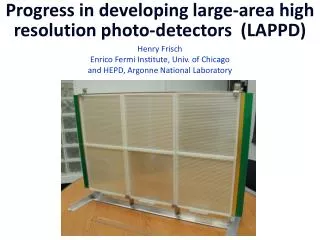
Micro-channel Plates Currently the glass substrate has a dual function- • To provide the geometry and electric field like the dynode chain in a PMT, and • To use an intrinsic lead-oxide layer for secondary electron emission (SEE) Micro-photograph of Burle 25 micron tube- Greg Sellberg (Fermilab)- ~2M$/m2- not including readout Argonne Alan Stone Visit
Get position AND timeAnode Design and Simulation(Fukun Tang) • Transmission Line- readout both ends=> pos and time • Cover large areas with much reduced channel account. Argonne Alan Stone Visit
Photonis Planicon on Transmission Line Board Couple 1024 pads to strip-lines with silver-loaded epoxy (Greg Sellberg, Fermilab). Argonne Alan Stone Visit
Comparison of measurements (Ed May and Jean-Francois Genat and simulation (Fukun Tang) • Transmission Line- simulation shows 3.5GHz bandwidth- 100 psec rise (well-matched to MCP) • Measurements in Bld362 laser teststand match velocity and time/space resolution very well Argonne Alan Stone Visit
Scaling Performance to Large AreaAnode Simulation(Fukun Tang) • 48-inch Transmission Line- simulation shows 1.1 GHz bandwidth- still better than present electronics. Argonne Alan Stone Visit
Proof of Principle • Camden Ertley results using ANL laser-test stand and commercial Burle 25-micron tube- lots of photons • (note- pore size may matter less than current path!- we can do better with ALD custom designs (transmission lines)) Argonne Alan Stone Visit
Measurements in ANL laser test-stand Jean-Francois Genat, Ed May, Eugene Yurtsev, + John Anderson, Karen Byrum, Gary Drake, Camden Ertley, Tyler Natoli Bob Wagner Argonne Alan Stone Visit
ANL Test-stand Measurements Jean-Francois Genat, Ed May, Eugene Yurtsev Sample both ends of transmission line with Photonis MCP (not optimum) 2 ps; 100 microns measured Argonne Alan Stone Visit
N.B.- this is a `cartoon’- working on workable designs- Large-area Micro-Channel Plate Panel “Cartoon” Front Window and Radiator Photocathode Pump Gap Low Emissivity Material High Emissivity Material `Normal’ MCP pore material Gold Anode 50 Ohm Transmission Line Rogers PC Card Argonne Alan Stone Visit Capacitive Pickup to Sampling Readout
Cartoon of a `frugal’ MCP • Put all ingredients together- flat glass case (think TV’s), capillary/ALD amplification, transmission line anodes, waveform sampling Argonne Alan Stone Visit
Mechanical Assembly sketch • Rich Northrop, Bob Stanek, HF, Michael Minot • Scalable in modules • Based on Ossy’s Planicon overall design • Strong industry involvement: Incom, CPS Technologies, MinoTek- adding others Argonne Alan Stone Visit
Can dial size for occupancy, resolution- e.g. neutrinos 4’by 2’ Argonne Alan Stone Visit
Plans to Implement This Have formed a collaboration to do this in 3 years. 4 National Labs, 5 Divisions at Argonne, 3 companies, electronics expertise at UC and Hawaii R&D- not for sure, but we see no show-stoppers Argonne Alan Stone Visit
Passive Substrates-1 • Self-assembled material- AAO (Anodic Aluminum Oxide)- Hau Wang (MSD) Argonne Alan Stone Visit
More CNM capabilities- Hau Wang-MSD Argonne Alan Stone Visit
Passive Substrates-2 Incom glass capillary substrate • New technology- use Atomic Layer Deposition to `functionalize an inert substrate- cheaper, more robust, and can even stripe to make dynode structures (?) Argonne Alan Stone Visit
Functionalization- ALD • Jeff Elam, Thomas Prolier, Joe Libera (ESD) Argonne Alan Stone Visit
Functionalization- ALD • Jeff Elam, Thomas Prolier, Joe Libera (ESD)
MCP Simulation • Zeke Insepov (MCSD) and Valentin Ivanov (Muons,Inc) Argonne Alan Stone Visit
MCP Simulation • Zeke Insepov (MCSD) and Valentin Ivanov (Muons,Inc) Argonne Alan Stone Visit
MCP Simulation • Zeke Insepov (MCSD) and Valentin Ivanov (Muons,Inc) Argonne Alan Stone Visit
MCP Simulation • Zeke Insepov (MCSD) and Valentin Ivanov (Muons,Inc) Argonne Alan Stone Visit
Nano-structured Photocathode Development Bernhard Adams, Klaus Attenkofer (APS); Mike Pellin, Thomas Prolier, Igor Veryovkin, Alex Zinovev (MSD); Jeff Elam (ES) Argonne Alan Stone Visit
Nano-structured Photocathode Development Argonne Alan Stone Visit
Nano-structured Photocathode Development Argonne Alan Stone Visit
Systematic Precise Characterization of SEE and PE for materials Mike Pellin, Thomas Prolier, Igor Veryovkin, Alex Zinovev (MSD) Argonne Alan Stone Visit
Systematic Precise Characterization of SEE and PE for materials Argonne Alan Stone Visit
Photocathode Development- Test setup at APS laser Bernhard Adams, Klaus Attenkofer, (APS), Matt Wetstein (HEP) Argonne Alan Stone Visit
Measurements of transmission-line anode in vacuum with photo-cathode and APS laser Bernhard Adams, Klaus Attenkofer, (APS), Matt Wetstein (HEP) Argonne Alan Stone Visit
Front-end Electronics/Readout Waveform sampling ASIC First have to understand signal and noise in the frequency domain EFI Electronics Development Group: Jean-Francois Genat (Group Leader) Argonne Alan Stone Visit
Front-end Electronics/Readout Waveform sampling ASIC EFI Electronics Development Group: H. Grabas, J.F. Genat • Varner, Ritt, DeLanges, and Breton have pioneered waveform–sampling onto an array of CMOS capacitors • All these expert groups are involved (Hawaii formally) Argonne Alan Stone Visit