Download
1 / 13
130 likes | 279 Views
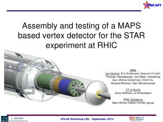
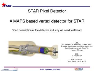
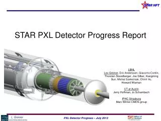
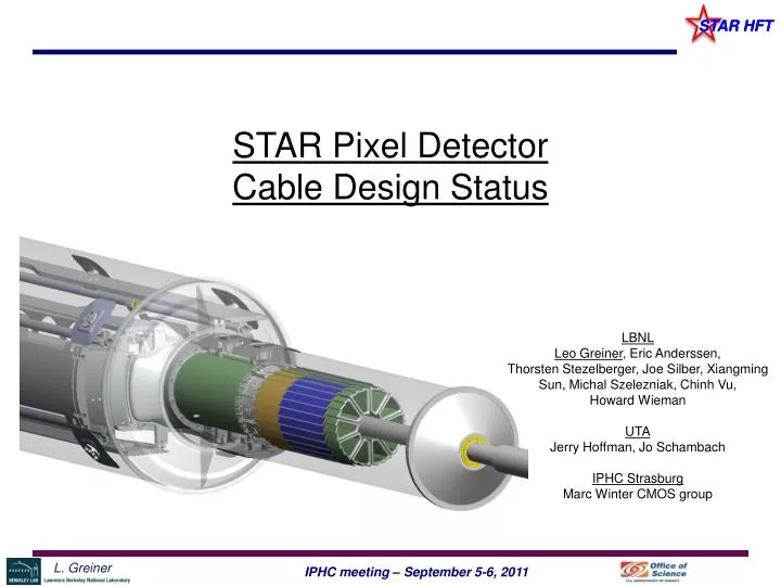
STAR Pixel Detector Cable Design Status. LBNL Leo Greiner , Eric Anderssen , Thorsten Stezelberger , Joe Silber, Xiangming Sun, Michal Szelezniak , Chinh Vu, Howard Wieman UTA Jerry Hoffman, Jo Schambach IPHC Strasburg Marc Winter CMOS group. Talk Outline.

E N D
STAR Pixel Detector Cable Design Status LBNL Leo Greiner, Eric Anderssen, Thorsten Stezelberger, Joe Silber, Xiangming Sun, Michal Szelezniak, Chinh Vu, Howard Wieman UTA Jerry Hoffman, Jo Schambach IPHC Strasburg Marc Winter CMOS group
Talk Outline • Prototype Design Concept • Current constraints from this version of Ultimate • Design choices based on above constraints • Current prototype design • Fabrication schedule
Cable Updated Status • We had originally intended to fabricate the prototype detector (end 2012 install) from Phase-2 sensors. • Ultimate is a success and we can change the plan to use Ultimate in the prototype detector. • This has ramifications for both the schedule, cost, development path for the cable, etc. • We will need to develop (Ultimate) probe testing earlier and change the cable design plans to design for Ultimate.
Cable Development PXL Cable development is planned as a 4 stage process: • Infrastructure testing board (large and configurable FR-4 ladder prototype). • - Validate design concepts and determine envelope of sensor operation. • Prototype detector cable FR-4 with Cu traces. • Prototype detector cable Kapton with Cu traces. • Prototype detector cable Kapton with Al traces. This process leads to a production Al conductor cable to be fabricated in the CERN PCB shops
Prototype Cable Design Concept Preliminary Design: Hybrid Copper / Aluminum conductor flex cable • 2 layer Al conductor cable with vias in low mass region • 0.004” (100 µm) traces and 0.004” (100 µm) spaces • 70% fill factor • Conductor thickness in low mass region is 21 µm (Cu) or 32 µm (Al) • Kapton thickness is 25 µm. • Bond wire connection between Al and Cu cable sections. • Cable size is approximately 2.3 cm x 28 cm. • We will design to this concept Low mass region calculated X0 for Al conductor = 0.073 % Low mass region calculated X0 for Cu conductor = 0.232 %
Signal path requirements The signal list with associated conductor count is shown below: *- these signals are required for prototyping and testing but can be removed on final production boards. It is desired to keep the trace resistance below 4 ohms to preserve signal amplitude. The sensor output and clock trace pair impedance should be approximately 100 ohms but 63 ohms has been shown to work satisfactorily in a similar data path design (the LVDS data path test, results may be found here (http://rnc.lbl.gov/hft/hardware/docs/LVDS/LVDS_test_report_1.pdf )
Existing Constraints from Sensor • High current draw on Analog power when the sensor is un-configured. • VCLP regulator yield. • Sensor start indeterminacy from START signal.
Proposed Design High current draw on Analog power (VDDA) when the sensor is un-configured. • Based on the results of the ITB tests, we will be implementing a single power supply for the VDDA and VDDD supplies for the sensors on the ladder. This makes sense as we wish to make the prototype cable as similar to the final cable as possible. • Implications: • RSTB implemented on cable to establish base sensor configuration before sensor power is applied. • Phased power application – driver section of cable is powered first, then sensors are powered after application of RSTB. These sections are on separate LU protected power supplies.
Proposed Design VCLP regulator yield • The current yield of the internal regulator for VCLP is of order 50% (is this still true?, cause?) • Options are to either accept the yield loss for the prototype detector and use sensors with functioning VCLP regulators or to provide a VCLP distribution bus. • The VCLP distribution bus adds conductor in a very congested area and is not foreseen to be needed for the production cable so we will design the cable without a VCLP distribution bus and accept the yield loss for this prototype. This also keeps the cable as close to production as possible.
Proposed Design Sensor start indeterminacy from START signal • There is a 1 clock indeterminacy in the sensor frame start based after the application of the START signal. • The options for dealing with this are to synchronize the application of the clock with the START signal or to do an alignment of the data in the firmware decoder used for receiving and sorting the data. • For technical reasons involving the way that we distribute the clock from the MTB, it is difficult to implement a solution involving the clock/start signal synchronous application. Also, this is expected to be solved in the final version of Ultimate. • We will implement a firmware alignment solution. • This solution is in progress.
Proposed Design SPEAK • As the frame boundary can now be checked for alignment based on the arrival of the frame header, the marker signal is not considered necessary for checking synchronization. • We intend not to bond the speak pads and disable them via RO_MODE4 Register - dis_pspeak. • Is this reasonable?
Current prototype design • We will produce a prototype cable design based on the design concept with a single 2 layer cable in the low mass region with wire bonded signals/power to the driver multi layer section. • This cable will use all copper conductors for the prototype. • Conductor list from the low mass region to the driver region:
Fabrication schedule • The schematic is complete and will be checked internally and by IPHC. • Layout will begin in mid-September. • We intend to have this cable fabricated in the CERN shops as a test of the capabilities and procurement path. • The design will be discussed with Rui at the CERN PCB shop in October when we are there for the beam test. • We expect the initial PCBs in the November - early December timeframe. • Does IPHC have any cable needs based on this design?