Download
1 / 57
570 likes | 803 Views
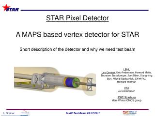
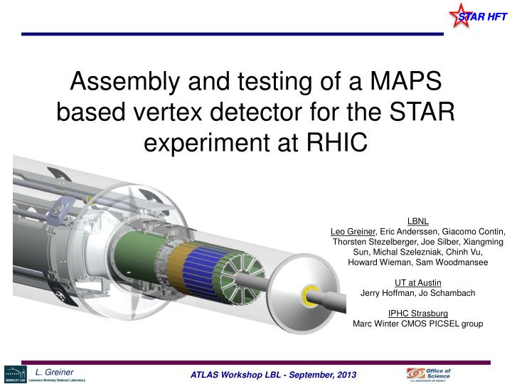
Assembly and testing of a MAPS based vertex detector for the STAR experiment at RHIC. LBNL Leo Greiner , Eric Anderssen, Giacomo Contin, Thorsten Stezelberger, Joe Silber, Xiangming Sun, Michal Szelezniak, Chinh Vu, Howard Wieman, Sam Woodmansee UT at Austin Jerry Hoffman, Jo Schambach

E N D
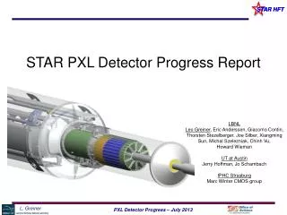
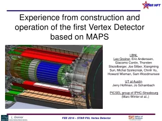
Assembly and testing of a MAPS based vertex detector for the STAR experiment at RHIC LBNL Leo Greiner, Eric Anderssen, Giacomo Contin, Thorsten Stezelberger, Joe Silber, Xiangming Sun, Michal Szelezniak, Chinh Vu, Howard Wieman, Sam Woodmansee UT at Austin Jerry Hoffman, Jo Schambach IPHC Strasburg Marc Winter CMOS PICSEL group
Talk Outline The primary focus of this talk is technical and on instrumentation. • Short overview of detector design. • Design of ladders, sectors, insertion mechanism. • Detector assembly, yields, integration and installation for engineering run. • In progress production, assembly and QA for the primary detector.
PXL in STAR Inner Detector Upgrades TPC – Time Projection Chamber (main tracking detector in STAR) HFT – Heavy Flavor Tracker • SSD – Silicon Strip Detector • r = 22 cm • IST – Inner Silicon Tracker • r = 14 cm • PXL – Pixel Detector • r = 2.7, 8 cm Direct topological reconstruction of Charm We track inward from the TPC with graded resolution: vertex ~1mm ~300µm ~250µm <30µm TPC SSD IST PXL
PXL Detector Requirements and Design Choices Requirements Design Choices • -1 ≤ Eta ≤ 1, full Phi coverage (TPC coverage) • ≤ 30 µm DCA pointing resolution required for 750 MeV/c kaon • Two or more layers with a separation of > 5 cm. • Pixel size of ≤ 30 µm • Radiation length as low as possible but should be ≤ 0.5% / layer (including support structure). The goal is 0.37% / layer (limits MCS) • Integration time of < 200 μs (limit pile-up, occupancy of ~250 hits/inner sensor) • Sensor efficiency ≥ 99% with accidental rate ≤ 10-4. • Survive radiation environment. • Air cooling • Thinned silicon sensors (50 μm thickness) • MAPS (Monolithic Active Pixel Sensor) pixel technology • Sensor power dissipation ~170 mW/cm2 • Sensor integration time <200 μs (L=8×1027) • Quick detector installation or replacement (1 day)
Aluminum conductor Ladder Flex Cable PXL Detector Design Mechanical support with kinematic mounts (insertion side) carbon fiber sector tubes (~ 200 µm thick) Insertion from one side 2 layers (tiled) 5 sectors / half (10 sectors total) 4 ladders/sector Ladder with 10 MAPS sensors (~ 2×2 cm each) 20 cm
PXL Detector Basic Unit (RDO) 11 m (24 AWG TP) 2 m (42 AWG TP) Mass Termination Board (signal buffering) + latch-up protected power Clk, config, data Clk, config, data, power RDO motherboard w/ Xilinx Virtex-6 FPGA 100 m (fiber optic) DAQ PC with fiber link to RDO board PXL built events • Highly parallel system • 4 ladders per sector • 1 Mass Termination Board (MTB) per sector • 1 RDO board per sector • 10 Sector chains in the PXL system Trigger, Slow control, Configuration, etc. Existing STAR infrastructure
Detector Characteristics 356 M pixels on ~0.16 m2 of Silicon
PXL Detector Highlights • The HFT upgrade to STAR received DOE CD-2/3 approval in September 2011 and became a construction project. • We installed a 3 sector engineering run detector into the STAR experiment on May 8, 2013 and ran the detector until June 10, 2013. • The production detector is scheduled to be installed in December of 2013. • We will build 2 complete detectors and enough good ladders to build a third. These serve as spares for rework if necessary. • I will give a brief overview of the PXL detector design details, components and assembly in the following areas: • Sensors • Ladder assembly and QA • Sector assembly and QA • Detector Half • Insertion mechanics • RDO System • Engineering run
Monolithic Active Pixel Sensors • Standard commercial CMOS technology • Room temperature operation • Sensor and signal processing are integrated in the same silicon wafer • Signal is created in the low-doped epitaxial layer (typically ~10-15 μm) → MIP signal is limited to <1000 electrons • Charge collection is mainly through thermal diffusion (~100 ns), reflective boundaries at p-well and substrate. • High resistivity epi for larger depleted region → more efficient charge collection, radiation tolerance. • 100% fill-factor • Fast readout • Proven thinning to 50 micron MAPS pixel cross-section (not to scale)
PXL detector Ult -1/2 Sensor • Reticle size (~ 4 cm²) • Pixel pitch 20.7 μm • 928 x 960 array ~890 k pixels • Power dissipation ~170 mW/cm² @ 3.3V • Short integration time 185.6 μs • In pixel CDS • Discriminators at the end of each column (each row processed in parallel) • 2 LVDS data outputs @ 160 MHz • Zero suppression and run length encoding on rows with up to 9 hits/row. • Ping-pong memory for frame readout (~1500 hits deep) • 4 sub-arrays to help with process variation • JTAG configuration of many internal parameters. • Individual discriminator disable, etc. • Built in automated testing routines for sensor probe testing and characterization. • High Res Si option – significantly increases S/N and radiation tolerance. Developed by IPHC, Strasbourg France
Ultimate 1 efficiency vs. fake hit rate Tested for STAR Operating conditions Marc Winter CMOS Group IPHC, Strasbourg, France Developed and tested by IPHC
Ladder assembly • Sector assembly • Half detector assembly
Ladder Design • Ladder assembly is the primary task for the detector fabrication. • We assemble ladders by edge bumping sensors on a vacuum chuck (the soft acrylic adhesive provides mechanical decoupling for CTE mismatches) • DRIE needed for precise sensor size. (most engineering run sensors were saw cut and this gave significant variations in the assembled length of the 10 sensor array, after DRIE, length variation in butted edge sensor array is ~50um) • Wire bonding is very sensitive to small sensor position variations (small displacements cause the bonding pads on the ladder to displace wrt bonding pads on the sensors and wire bonds then require steep angles).
Ladder Design Ladder cable concept
Ladder assembly work flow chart Electrically tested driver boards Dimensionally checked compositebacker Probe tested sensors Electrically tested low mass cables Ladder assembly • Ladder characterization • Reworking and troubleshooting • Quality assessment • Initial validation Ladder wire bonding 1 day without problems Full functionality test Wire bond encapsulation • Full functionality test • bias optimization • Threshold scan • Normal readout mode test • Accidental hit rate scan Quick test Complete ladder • Quick test • Threshold scan @ nominal bias settings
Sector/half-detector work flow chart machined Dovetail/D-tube Elect tested MTB/cables/insertion Tested Ladders Sized Sector Tubes Sector assembly Quick test Sector metrology Quick test Half detector head assembly Half detector head metrology Full Half detector assembly Quick test Full functionality test ½ HFT PXL
Overall detector design factors (metrology) • We intend to insert a fully mapped detector with all pixel positions known and stable. • We have gone to great lengths to ensure that the ladder/sector/half detector mechanics are stable to 30um for all forces (gravity, vibration and deflection due to air cooling (~10 m/s), thermal distortion, mechanical stress from cable loading, etc.) anticipated during running. • We map each sector using fiducials on the sensors and relate pixel positions to tooling balls on the sectors. • We then assemble half detectors and map the sector tooling balls to give the pixel positions for each half detector.
Sensor Thinning • We use sensors thinned to 50 µm thickness. • We use DRIE processing on the wafers to give accurate sensor dimensions and edge quality. • Wafers are delivered with DRIE trenches 70 µm deep. The wafers are back-thinned and polished at Aptek to release the dies from the wafer (yield started quite low, but is now significantly improved). • First 25 production wafers, 5 were lost completely during thinning as process was refined. Last 17 wafers thinned had >99% yield. • Die position on the wafer and wafer # are preserved through the thinning process and this identifies the die in our database. • We select dies based on probe testing of thinned sensors. • 50 um thick sensors are curved, up to 2 mm out of plane, this has implications.
Assembling sensors into ladders – Probe Testing Yield modeling makes probe testing critical to the goal of assembling functional 10 sensor ladders. We test thinned and diced 50 µm thick sensors (curved). This is not easy. • Probe card with readout electronics • derived from individual sensor test card • Analog and digital sensor readout • Full speed readout at 160 MHz • Full sensor characterization at full speed • Test results used for initial settings in ladder testing and PXL detector configuration • 2nd generation probe card for production testing • only digital readout pins loaded
Assembling sensors into ladders – Probe Testing • Vacuum chuck for testing 20 thin sensors (50 µm) • Thin sensors are sensitive to chuck surface imperfections • Need a special probe pin design and to work in clean environment • Testing up to 18 sensors per batch • Optimized for sensor handling in 9-sensor carrier boxes • Manual alignment (18 sensors ~ 1 hr) • Testing time is ~ 15 minutes per sensor (3 supply voltages) (4.5 hr testing time) Threshold DAC counts (x5) Discriminator Threshold LabWindows GUI Column number
Examples of failures E05_w_08 C04_w_12 OK D07_w_12 Faulty columns Sub-arrays E01_w_8 (@3.0V) E05_w_12 Faulty rows 3.3 or 3.0 V E06_w_12
Automated interface to a database (18 config + 68 result parameters) Sensors are binned according to performance PXL Sensor selection Example of wafer maps for Ultimate-2 wafers with DRIE processing (ion etching) ~65% - 70% yield (Tier 1-3) 40% Tier 1-2
Assembling sensors into ladders – Hybrid Cable • The cable is needed to deliver power and ground and provide signal routing to and from the sensors on the ladder with minimal radiation length. • Production aluminum conductor flex cables are being fabricated in the CERN PCB shop. (difficult to produce, only one real vendor) Hybrid Copper / Aluminum conductor flex cable design concept • 20 differential signal output pairs • JTAG, 2 temp diodes, CLK, START • VDD, VDA, GND - ~1.8 A / ladder Layout (in copper) Low mass region calculated X/X0 for Al conductor = 0.079 % Low mass region calculated X/X0 for Cu conductor = 0.232 %
Assembling sensors into ladders – Assembly Reference pins for cable/sensor alignment • We use precision vacuum chuck fixtures to position sensors and assemble ladders. • Sensors are positioned with butted edges. Acrylic adhesive mechanically decouples sensors from the cable and prevents CTE difference based damage. • Weights taken at all assembly steps to track material and as QA.
Assembling sensors into ladders – Assembly • Hybrid cable with carbon fiber stiffener plate on back in position to glue on sensors. • The cable reference holes are used for all aspects of assembly of ladders and sectors.
QA/QC for Sector Production Assembled ladder with driver board, wire bonded and encapsulated Completed ladder in anti-static carrying box with follower and check off list.
Engineering Run Ladder Yield • The assembly of ladders and sectors for the PXL Engineering Run has been crucial for process optimization and we have dealt with a number of unexpected issues. • Thanks to this experience, we were able to refine the assembly procedure and to develop effective tools for troubleshooting ladders. • The final ladder assembly statistics for the engineering run detector are: • The primary lessons learned had to do with the need for coverlay on the cable, modification of tooling that was damaging sensors, adjustment of adhesive sizes and backing plates, proper adjustment of sensor array on the cable.
Ladders to sectors Sector in optical metrology machine • Sensor fiducial positions on sector are measured optically and related to tooling balls. • Surface profiles of sensors (sensors are not flat) are measured using feather touch probe CMM and pixel positions are related to sensor fiducials using thin plate spline fit. Now we have pixel positions related to the tooling balls. • After touch probe measurements, sectors are tested electrically for damage from metrology.
sectors to detector half (ER) • Sectors are mounted in dovetail slots on detector half. • Metrology is done to relate sector balls to each other and to kinematic mounts. We now have pixel positions for the half detector object.
Mechanical Development Air-flow based cooling system for PXL to minimize material budget. ladder region • Silicon power: tested at 170 mW/cm2 (~ power of sunlight) • 350 W total in the ladder region (Si + drivers) Detector mockup to study cooling efficiency computational fluid dynamics
Mechanical Development 340 W with ambient air = 26.8 C unsuported end mid-section fixed end Solid – inner layer Open – outer layer • Measurement results agree with simulations and meets calculated stability envelope tolerance. • Air flow-induced vibrations (10 m/s) are within required stability window. NTC thermistors (averaged at same “Z” position) Thermal camera image of sector 1 (composite image): Power ~340 W Airflow 10.1 m/s
PXL detector – insertion mechanics • Unusual mechanical approach. • Cantilevered and insertable (1 day) • Pre-surveyed and mechanically stable to a level that preserves the survey. • Detector inserts and initiates a clamshell closing around beam pipe, and is locked into position on kinematic mounts.
PXL insertion mechanics Interaction point view of the PXL insertion rails and kinematic mount points Carbon fiber rails Kinematic mounts
PXL insertion mechanics PXL detector half with complete insertion mechanism
Engineering Run Left detector half being inserted Right detector half being inserted
Engineering Run PXL eng detector inserted, cabled and working in 1 day access
Engineering Run • PXL system working with 3 sectors • Integrated with STAR trigger, DAQ, slow controls, online event pool. • Software and firmware for performing data quality checks were modified and optimized. Hit display for PXL engineering run detector.
Preliminary results from Engineering Run First tracking results show good matching of TPC tracks to hits on PXL sensors Residuals compatible with TPC track resolutions on the sensors (~1-2 mm) 3mm beam shift reflects the PXL&TPC relative position
Lessons learned • “Full dress rehearsals” are critical to success. • We discovered a mechanical conflict in the ladder driver board section that necessitated a sector tube redesign. • Tooling that would fracture sensors during assembly was modified. • Our ladder temperature monitoring system didn’t work properly and was re-designed. • Other electronics / sensor issues are still under investigation and will require further updating of the existing systems.
Production detector • We are currently building ladders for the production detector. • Mechanical thinning yields are now close to 100%. • Current ladder yields are much better. • 36 ladders produced, 26 tested, 1 ladder has 1 damaged sensor, all others tested are fully functional. • Production sector assembly will start in mid-September.
Read-out Electronics The detector is 10 parallel sector chains. Each sector is configured and delivers data to the RDO boards continuously into a data pipeline. The receipt of a trigger opens an event buffer for 1 frame of data. (2 actual frames with address selection performed to give one compete frame based on the time the trigger is received) The data is formed into an event and shipped to the DAQ receiver PCs. Full PXL RDO fits into 1 crate