Download
1 / 31
310 likes | 312 Views
This overview discusses the modifications made to the layout and design of the pixel detector, including the introduction of the "insertable concept" for easier maintenance and upgrades. It also covers the coverage, material, and performance of the detector, as well as the integration of services and mechanics.

E N D
Pixel Detector Status ATLAS Collaboration Meeting BNL June 5, 2001
Overview Layout Coverage Material Performance Insertable Concept Services Integration Mechanics Modules and Hybrids Sensors Electronics Critical Points Over Next Year Outline
Overview • Pixel detector layout and design have been modified over about the last nine months to cope with delays in radiation-hard, integrated circuit electronics. • Complete pixel detector can be inserted or removed with remainder of Inner Detector in place ie. as late as possible for initial installation. • This required modifications to the pixel layout(reduction in active area), changes to the SCT disk layout(detectors), introduction of a pixel support tube with rails and major changes to the services routing and integration of the pixel detector. • This “insertable concept” will also facilitate maintenance/repair and upgrades.
Layout Can provide 3 hits for ||2.5 Three disk layers Three barrel layers Pixel size is 50x400, except for innermost barrel layer that is 50x300
Coverage 50 GeV Muons • Geometric losses re-evaluated recently. • Losses from clearances(barrel), inability to get first disk close enough to barrels, small gaps at outer radii of disks.
Material • Comparison of insertable-baseline(red) with previous layout(blue). 3 hits. • Comparison of insertable-baseline(now blue) with option of B-layer services exiting both sides(red). 3 hits. • Two-hit system ie. possible initial detector.
Performance • Parametric performance of insertable-layout is similar to previous layout, and yields parametric performance about same as that assumed in Physics TDR. • Routing of services along support tube => increase material relative to previous layout. • Studies of impact on EM calorimeter resolution, track finding/fitting and b-tagging underway. • Goal is to have results for LHCC review early next month.
Insertable Concept • Pixel system and services roll into support tube held by SCT barrel and at ends of ID. • Services for all but innermost(B-layer) go out both sides. • B-layer exit services on one side, since must be installed with beam pipe in place, from one end(current baseline). • Beam pipe to be integrated into pixels on surface and then pixels+beam pipe delivered as package to end of support tube. Pixel support tube is held by SCT barrel and at both ends to cryostat. Details of these interfaces are being designed. Pixel Support tube Patch PPF1 PPB1 No Longer Used PP1 Inner Tracker Section Pigtail All Cables run along the Support Tube and then to PP2. Pixel Volume PP0 Location
Insertable Pixels - General Requirements • Complete pixel detector installation to be done in “long access” now renamed “IDET removal” configuration. • Installation of B-layer without breaking beam pipe vacuum is required. The pixel group has requested consideration of alternative wherein the B-layer must be installed together with the rest of the system/beam pipe on the surface. This improves significantly the B-layer services design, reduces some material in the active region and the large X0 peak just above = 2.5. And reduces the time spent in radiation field(from beam pipe, ID, etc). • Beam pipe bakeout can be done with the B-layer in place. However, this will not be confirmed until passing Eng. Design Review of the beam vacuum system anticipated to occur end of 2001. • Pixel system + beam pipe to be assembled on surface, lowered as a package and rolled into the pixel support tube. • Design of pixel support tube allows for X or Y motion of the beam pipe relative to ATLAS by up to 9mm(with access to the ends of the support tube).
Support Tube - Composite Structure 0.44 mm wall 7.5m long Bolt flanges Sct mount pads End Plugs for services feedthroughs and to hold ends of tube round.
Mockup • Complete mockup of support tube, pixel components and beam pipe needed. • Support tube part is essentially complete(at LBNL). • Other components in fabrication or design. • Study assembly/installation steps in detail. Essential to understand schedule as well as validate design concepts. Service Rails Detector Rails
Services Integration - Internal Pigtail(electrical) connections from each module to Patch Panel 0 Barrel and disk services both sides 6X 7X Patch panel 0 Electrical-to-optical transition 580 495 650 B-layer services exit one side of ID Service panels hold cables, pipes and fibers Structure necessary to support services during installation. These slide along rails in support tube
Service Integration - External • Implication of recent “gap decision” is that pixels can just retain present concept for power and signal cables IF current allocated volume is kept. May increase cable costs in region PP1 to PP2. • However, voltage regulation(rad-tolerant) at PP2 is required and it is not clear if this will work with PP2 not in gap region(longer distance) but no room for PP2 in gap. • Although some evaluation of feasibility will be done with next generation of rad-tolerant regulators and dummy loads, a real answer requires testing active modules with 0.25 micron FE chips. This cannot be done until early 2002. • Significant uncertainties in external cable and patch panel layout will exist until these tests are complete next year. Tube Flange EMI foil on support tube To pp2 Service Panels Bulkhead feedthroughs “cable trays” from pp1 to pp2 region for EMI shielding PP1 region Double wall beam pipe EMI foil on beam pipe
Mechanics - Local Supports Aluminum tubes for coolant • Barrel staves and disk sectors are Local Supports that hold and cool pixel modules. • Many prototypes of Local Supports made. • Production Readiness Review for Local Supports and Conceptual Design Review of rest of mechanics next month. Carbon-carbon for support and heat conduction Disk Sector Bi-stave Assembly Aluminum tubes for coolant
Mechanics - Intermediate Supports • Two disk ring support prototypes made, prototype sectors attached and design evaluated extensively. • Disk support ring design completed, design of fabrication tooling in progress. Prototype barrel half-shell 2nd prototype disk support ring • Barrel shell prototype made, dummy loads applied, extensive measurements. • Barrel shell design well advanced.
Mechanics - Global Support Disk Sections • Frame prototype made and design well advanced. • Barrel support cone prototype complete next month. • Trial insertion of disk ring into prototype of frame started. Barrel Section Barrel Support Cone
MCC Front-end chips Kapton hybrid Kapton hybrid glued to sensor Modules • Bare module(sensors bump bonded to front-end electronics) FDR completed August 2000. • Work in progress to make 50 dummy modules/per each of two bump bonding vendors this year, in addition to assembly of some active modules. Key goal to validate 8” wafer capability. • Flex hybrid FDR completed December 2000. 3rd generation prototype design completed and vendors being selected. Design modified to allow more potential vendors to bid.
Module Assembly and Placement Stave Module Placement Tooling • Ongoing program with mechanical dummies to develop tooling for attaching flex hybrid to bare modules and placement of completed modules on Local Supports. • Preliminary tooling complete for both barrel and disks, modifications to be made as we gain experience. • Extensive characterization of adhesives for attachment is ongoing, including irradiation. Disk Sector Module Placement Tooling
Optical Hybrids DORIC PIN -> electrical VDC Drive VCSEL Pixel Volume PP0 Location 1st Optical Hybrid Prototype 2cm Optical fibers PP0 Printed Flex Prototype Optical package(VCSEL and PIN diode) 2cm Modules plug in here - electrical to optical transition
Optical Components • Optoelectronics(DMILL) were irradiated recently at PS (lifetime dose is expected to be about 35 Mrad). • Online results were mixed for DORIC and VDC. 3-4 of each were tested, some failed before lifetime dose, some did not. Tests to be done after annealing to more accurately simulate real conditions. Insufficient data so far to reach conclusion about viability of DMILL. • Optical hybrid also irradiated. Different optical packages tried, also two types of VCSELs. Again results mixed. At about 6 Mrad, reduced light from VCSELs gives error rates but found design deficiency in receiving board that complicates understanding. • Pixel optical system review next week. • Bottom line. Need more tests. 2nd generation optical hybrid board fabrication underway, improved diagnostics(receiver board) for error rate measurements, focus on single optical package design after next week.
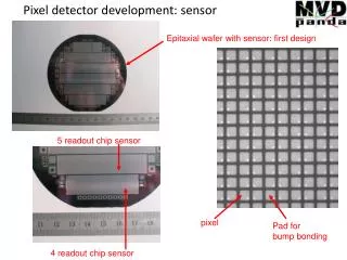
Sensors • Baseline design is n+ pixels in n-bulk material(double-sided processing), p-spray isolation of n+ implants, with bias grid to allow testing before module assembly and uses oxygenated silicon to improve radiation resistance and increase allowable time at “room” temperature(for repair or upgrades). • PRR completed February 2000. • Preproduction launched with two vendors CIS and Tesla. Contract specifies minimum yield values for module sensors(tiles). • CIS preproduction complete. Test results so far show good quality and excellent correlation between our QC measurements and those done by CIS. • Only limited results so far for wafers from Tesla. They have had yield problems, but believe these are now solved. More wafers will arrive for testing in next month or so.
Electronics - Overview • Four rad-hard ICs needed. Radiation hardness up to about 50 Mrad and 1015 n/cm2 • FE chip, 16 per module • MCC, event builder for 16 chips on a module, data-in, data-out, clock. • VDC(VCSEL Driver Chip) to drive data off-detector. • DORIC to decode/encode clock and control. FE MCC DORIC VDC
Electronics - Short History • Rad-soft FE and MCC development successful and used for module testing, irradiated sensor testing…demonstrating that ATLAS specifications could be met. • Rad-hard FE development began with Atmel/DMILL in mid-’98 and first submission was in Aug. ‘99. These (FE-D1) chips had very poor yield, traced laboriously to technology problems. • Second run with Atmel submitted in July ‘00 and included two versions of FE(FE-D2D and FE-D2S) + MCC, VDC and DORIC prototypes. FE-D2D like FE-D1 with bug fixes. FE-D2S modified design to remove circuit elements sensitive to technology problems but at cost of removing some important functionality to remain with 400 micron long pixels. • Yield of FE-D2D like FE-D1 ie. essentially zero. Yield of FE-D2S good enough to continue evaluation and to proceed to build a few active modules, which are nearing completion. MCC yield low(10% or so). VDC and DORIC promising. • Honeywell design work abandoned in Aug. ‘00 after large price increases. • FE-D2S irradiated(high dose rate) in Feb. ‘01. On-line results bad(ie. chips died) but functionality returned after annealing albeit with performance changes. • Design work stopped for FE and MCC in DMILL in Sept. ‘00 and all effort concentrated on 0.25processes. 0.25 and DMILLdesign work on VDC/DORIC continuing.
Two pixels (analog) in DMILL 50 Two pixels in 0.25 50 0.25 Design • Dual process approach with TSMC/IBM, production with IBM but rapid prototyping with TSMC also available via MOSIS each month. • First digital test chip submitted to TSMC in Jan. ‘01. Limited functionality but worked roughly as expected. • Analog test chip submitted to IBM and TSMC in Feb/Mar ‘01.
Analog 0.25 Test Chip • Analog test chip contains preliminary designs of analog blocks. 20 pixels. Other critical analog items. Nominally final layout of critical items. • TSMC chip delivered May 15. • Rapid preliminary evaluation using “portable” test system complete. • IBM version(identical) will arrive very shortly and tests will begin next week at CERN during Pixel Week.
Analog Test Chip Irradiated • 1st irradiation with 55 MeV protons on May 26 at very high dose rates(up to 10 Mrad/hr) at LBL cyclotron. • On-line results indicated little or no change in performance(noise, timewalk,…) after 50+ Mrad as do preliminary tests done after irradiation. • Example below is post-radiation timewalk performance(left and right plots taken at different times, absolute scales different. T between high Q and low Q is relevant). • Additional characterization and irradiation(55 MeV and at PS) of both TSMC and IBM. • Results encouraging but still early in evaluation process. Irradiation with 55 MeV prototons
First 0.25 Engineering Run • Integration and verification of first full FE chip for engineering run advanced. • Design review this week at CERN. • Goal is to submit 12 wafer run next month. • Integration and verification of MCC chip progressing in parallel. First MCC prototype in 0.25 also to be included in this run. • 0.25 prototypes of optical ICs already submitted to IBM multi-project run in February but will also be included in engineering run. • Planned wafer arrival by November this year. First complete 0.25 chip set.
Unified Test System • A second generation test system is nearing completion and will be finished later this year for distribution throughout collaboration. • Allows (FE) IC wafer probing, test board evaluation, bare module probing and assembled module testing to be done with unified system(and software) across the collaboration. • Significant capability needed to test, for example, modules that each have about 50K channels. • Essential to make rapid, coherent progress.
slave DSPs & memories power supplies program FLASH boot FPGA ROD bus buffers router FPGAs event builder FPGA controller FPGA debug & derandomizing memories master DSP & memory dataformatterFPGAs realtimedatapath ReadOut Driver Prototype • SCT/Pixel RODs are joint development. Current emphasis on SCT but pixels are variant of same basic board. • SCT prototypes made and under test. Pixel FDR in 2002.
System Tests • Rudimentary system tests starting. • Adding active modules, rad-soft vintage, to local(disk) supports. • Limited by availability of active modules. • If FE-D2S modules are useful, can also be mounted. • Next step is to test services chain up to power supplies. Active module on disk sector. Two additional rad-soft modules to be added shortly.
Critical Points Over Next Year • Complete transition to insertable pixel system as baseline • Finish performance studies and ECR • Beam pipe review -> favorable to in situ bakeout with B-layer in place? • Require B-layer in-pit insertion or only on surface? Activation/radiation. • Better understanding of assembly/installation tasks/schedule • Front-end integrated circuit remains critical path item. Complete evaluation of 1st prototypes, launch 2nd iteration. • Assuming 1st ICs successful, expand multi-module system tests on Local Supports. • Services integration - complete full prototype chain from module to power supply(including regulators). • Begin production of sensors, Local Supports and other parts of mechanics.