Download
1 / 13
130 likes | 285 Views
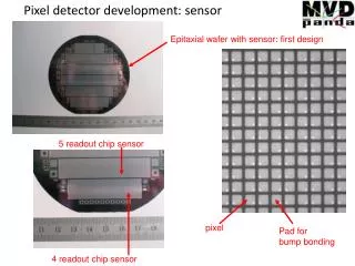
BTeV Pixel Detector. Data In and Out project. Optical link receiver chip. Data In Out. Is the interface between the Pixel Detector and the pair DAQ system/Trigger processor. Ships pixel hits generated by the FPIX chips at high speed (~16Gb/s/plane).

E N D
BTeV Pixel Detector Data In and Out project Optical link receiver chip
Data In Out • Is the interface between the Pixel Detector and the pair DAQ system/Trigger processor. • Ships pixel hits generated by the FPIX chips at high speed (~16Gb/s/plane). • Accepts Initialization, Control and timing information for the FPIX chips. • Provides clean clocks for FPIX and Tx chip. • Optical links will be used for input and output links
Data In Out requirements: • Must fit in a tiny space at the corners of the Pixel planes. • Radiation hardness: 1 Mrad • Low Power budget: 1 W/corner • Low material budget: no ferromagnetics. • Everything must operate in the vacuum. • EMI noise resistant.
Optical link receiver chip goals: • Initialize FPIX chips • On line control FPIX chips • Generate appropriate timing for FPIX • Some on line control to the Data Concentrator chip • Supply clean clocks
Optical link characteristics: • VCSEL: Ithmin=5mA, Opt. Power: 1mW (min). • PIN: responsivity 0.3 A/W. • Optical Receiver: Current to voltage front-end amplifier. • Cost: > $150/fiber: • VCSEL: $35 • PIN: $35 • Rad hard fiber: $3.5/m total(10m): $35 • Standard fiber: $0.15/m total(150m): $22.5 • Connector/Assembly: MT12 $80/pair, ~$15/fiber. • Total cost per extra fiber in the Pixel Detector (~200 planes): $30K. Moral: minimize the number of fibers.
Input Data characteristics: • Three clocks: • Readout clock: 53 MHz, external. Needs jitter<100-150ps • BCO clock: 7.56 MHz, external. • FPIX Initialization clock (ShiftIn): few MHz needed. • Initialization and Control data speed: few MHz needed. • Initialization and Control data/clock are not concurrent. • Conclusions: • Data can be serialized • 53MHz clock and ShiftIn can share the same channel. • Both clocks and data can share the same channel
Single fiber for clock and data. Guarantied transition every clock cycle. DC balanced. Self clocking. Data and clock onto a single fiber (1) • Figure: (upper) Bi-Phase mark encoding (lower) Manchester encoding
Data Frame: • Start: frame synchronization • Command: internal acction on FFs and logic. • Data: Init. Data for Fpix chips.
Optical Receiver chip specifications: • Input signals: PiN signal is AC coupled to comparator. Input power about 1 mW. PiN responsivity > 0.3A/W. • 53 MHz clock jitter: 100-150ps • Output signals: CMOS and LVDS to the FPIX chip • Noise: as a function of BER. For instance: 10^-12 for the channel after irradiation => S/N > 15. We probably need S/N > 20 at the receiver. • Radiation: 10^13 n/cm² plus 1Mrad maximum estimated. • Physical size: must fit in 7 cm². The area is not rectangular but with an ugly shape. Unless the mechanical specification of the Pixel Plane changes. • Temperature: -20C to 30C ? • Vacuum:
Some questions: • Will the receiver input need a PLL? • Can IC tap delays be as accurate as required for the 106 MHz data case over time, temperature variations & accumulated radiation effects? • How is a frame error detected remotely? Is it really necessary to detect frame errors. Won’t the system let you know of some error if framing is lost. • Do startup problems arise (e.g., due to capacitor charge up times) if the receiver’s input signal is turned off for a brief period? Is it better to have the receiver check for a unique 14-bit data pattern (e.g., all ones) for proper framing detection? • How does the slow control system get control data back from Denes’ ICs if that is the path for read-back of control/downloading information?