Download
1 / 47
470 likes | 474 Views
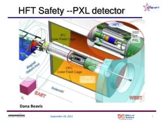
HFT PIXEL Detector. Pre-practice CDR-1 Review 3-Sept.-2009 Wieman. Topics. Pixel detector system requirements and properties detector chip and readout development Mechanical development. Pixel geometry. These inner two layers provide the projection precision. End view. 8 cm radius.

E N D
HFT PIXEL Detector Pre-practice CDR-1 Review 3-Sept.-2009 Wieman
Topics • Pixel detector system requirements and properties • detector chip and readout development • Mechanical development
Pixel geometry. These inner two layers provide the projection precision End view 8 cm radius 20 cm 2.5 cm radius Inner layer Outer layer coverage +-1 One of two half cylinders total 40 ladders
Some pixel features and specifications critical and difficult more than a factor of 2 better than other vertex detectors (ATLAS, ALICE and PHENIX)
Monolithic Active Pixel Sensors MAPS pixel cross-section (not to scale) Detector chips developed by Marc Winter’s group at IPHC in Strasbourg, France • Standard commercial CMOS technology • Only NMOS transistors inside the pixels • Room temperature operation • Sensor and signal processing are integrated in the same silicon wafer • Signal is created in the low-doped epitaxial layer (typically ~10-15 μm) → MIP signal is limited to <1000 electrons • Charge collection is mainly through thermal diffusion (~100 ns), reflective boundaries at p-well and substrate → cluster size is about ~10 pixels (20-30 μm pitch) • 100% fill-factor • Fast readout • Proven thinning to 50 micron
Sensor generation and RDO attributes Gen Sensor Sensor RDO Mimostar–2 30 µm pixel, 128 x 128 array 1.7 ms integration time 1 analog output Mimostar–3 30 µm pixel, 320 x 640 array 2.0 ms integration time 2 analog outputs Phase–1 30 µm pixel, 640 x 640 array 640 µs integration time, CDS 4 binary digital outputs Final (Ultimate) 18.4 µm pixel, 1024 x 1088 array ≤ 200 µs integration time, CDS, zero suppression 2 digital outputs (addresses) 50 MHz readout clock JTAG interface, control infrastructure ADCs, FPGA CDS & cluster finding zero suppression ≤ 4 sensor simultaneous readout 160 MHz readout clock JTAG interface, control infrastructure zero suppression 120 sensor simultaneous readout 150 MHz readout clock JTAG interface, control infrastructure 400 sensor simultaneous readout (full system) 1 DONE 1 2 PROTOTYPED 3
Silicon development • Phase 1 • for use in the engineering run • on pixel CDS • on chip discriminators • binary hit read out • integration time 640s • Ultimate • for full installation run • functionality of Phase 1 plus zero suppression • integration time <200 s – suitable for full luminosity operation
HFT PIXEL MAPS 120 GeV π- beam test at CERN M.i.p. detection performances of a 100 μs read-out CMOS pixel sensor with digitised outputs – Marc Winter et. al., http://arxiv.org/PS_cache/arxiv/pdf/0902/0902.2717v1.pdf CMOS pixel sensor development: a fast readout architecture with integrated zero Suppression – C. Hu, PIXEL 2008 Efficiency and Fake hit rate for Mimosa-22. This sensor has the same design as the final HFT Pixel sensor. This sensor has been tested to 150k rad and maintained 99.5% efficiency with < 10-4 fake hit rate. Efficiency and Fake hit rate for Mimosa-16. 25um pixels at 20º C. This is the sensor design that is the basis for the HFT Phase-1 Pixel sensors.
Phase - 1 • Extensively tested and characterized by the LBNL group • Multiple chips have been studied doing scans of operating parameters to determine optimum operation mode and determine permissible operation limits • Readout, firmware, testing tools mature, ready for probe testing of diced and thinned chips • so far ~100% yield of chips sampled from different locations on the wafer • Noise levels suitable for engineering run, but potential improvements have been identified and a second run is planned • near future – build a multi chip telescope and test in a minimum ionizing beam
Phase-1 – full reticle binary output prototype 640 x 640 pixels, 30 um pitch, 160 MHz RDO clock, column level discriminators, 4 binary outputs, 640 us integration time Digital output Analog output Phase-1 prototype on testing board. Initial observations of Phase-1 operation Phase-1 prototype sensors have been fabricated and tested at LBNL
Example parameter scan (Vref2) Chip D1 (parameter scan) VREF2 = 81 0.887 V VREF2 = 82 0.898 V VREF2 = 83 0.909 V VREF2 = 84 0.920 V VREF2 = 85 0.931 V (@ ICLPDISC = 80) Discriminator threshold voltage identified by 50% pixel hits (half below threshold half above threshold) Mean noise value Threshold dispersion (one half of the chip seems to be sensitive to the parameter value) issue to be studied further at IPHC to understand cause
Ultimate status • design is nearing completion • will be submitted for first fabrication Feb 2010
Readout studies: LVDS Data Path Testing http://rnc.lbl.gov/hft/hardware/docs/LVDS/LVDS_test_report_1.pdf • Significant test of system data path at up to 200 MHz with 3 streams of pseudo-random data • Xilinx Virtex-5 IODELAY element allows fine tuning of all individual input latching in 75 ps increments. Only system jitter affects data latching. • Measured BER (bit error rate) of <10-14 for 1 m 42 AWG and 6 m twisted pair data cables at 200 MHz and for 2.3 m 42 AWG at 160 MHz. • The RDO system architecture is considered to be validated and we then worked on the design of the full functionality prototype system. Ladder mock-up with 1-to-4 LVDS fanout buffers 42 AWG wires Mass termination board + LU monitoring 24 AWG wires 2 ns eye pattern opening for 1 m 42 AWG cables at 200 MHz Virtex-5 based RDO system with RORC link to PC
current readout development work • Preparing for probe test • Develop multi chip readout capability (a modification of the current system)
HFT PIXEL mechanical development • Stability analysis • Thermal analysis • Air flow vibration tests • Thermal tests • Fabrication development • Installation mechanics
r1 r2 perceived vertex true vertex m x x v v r1 r2 perceived vertex true vertex vertex projection from two points expectations for the HFT pixels pointing resolution = (13 22GeV/pc) m first pixel layer from coulomb scattering from detector position error more than 3 times better than anyone else detector layer 2 detector layer 1
Mechanical Stability Once the pixel positions are measured will they stay in the same place to within 20 µm? Issues that must be addressed: • Movement from temperature changes • Movement from humidity changes • Deflection from gravity • Movement induced by cooling air (to be addressed after thermal discussion) • how much air is required • vibration and static displacement
Stability requirement drives design choices • The detector ladders are thinned silicon, on a flex kapton/aluminum cable • The large CTE difference between silicon and kapton is a potential source of thermal induced deformation even with modest 10-15 deg C temperature swings • Two methods of control • ALICE style carbon composite sector support beam with large moment of inertia • Soft decoupling adhesive bonding ladder layers
cable bundle drivers kapton flex cable pixel chips adhesive composite backer adhesive wire bonds capacitors Ladder design with soft adhesive (6 psi shear modulus) adhesive: 3M 200MP 2 mil, film adhesive
FEA analysis of thermally induced deformation of sector beam • FEA shell elements • Shear force load from ladders • 20 deg temperature rise • Soft adhesive coupling • 200 micron carbon composite beam • end cap reinforcement • Maximum deformation 9 microns (30 microns if no end cap)
FEA analysis - sector beam deformation – gravity load • FEA shell analysis • 120 micron wall thickness composite beam • gravity load includes ladders • maximum structure deformation 4 microns • ladder deformation only 0.6 microns
Air cooling of silicon detectors - CFD analysis • Silicon power: 100 raised to 170 mW/cm2 (~ power of sunlight) • 350 W total Si + drivers air flow path – flows along both inside and outside surface of the sector
Air cooling – CFD analysis stream lines with velocity • air flow velocity 9-10 m/s • maximum temperature rise above ambient: 12 deg C • sector beam surface – important component to cooling • dynamic pressure force 1.7 times gravity silicon surface temperature velocity contours
The message Lots of complicated modes close in frequency End cap raises frequencies a bit vibration modes with reinforced end cap 259 Hz 441 Hz 276 Hz 497 Hz 397 Hz
wind tunnel setup to test vibration and displacement carbon fiber sector beam capacitance vibration probe two positions shown air in air out adjustable wall for air turn around air velocity probe two positions shown C:\Documents and Settings\Howard Wieman\My Documents\aps project\mechanical\PXL phase 1 sept 2008\sector ph1 wind tunnel.SLDASM
Ladder vibration induced by cooling air no reinforcement at the end system resolution limit all errors desired vibration target
17 µm 17 µm 6 µm -167 µm 9 µm -179 µm 11 µm -248 µm 1 µm -156 µm -163 µm -113 µm measured static deformation from 9 m/s air flow open end reinforced end
4 µm 6 µm 6 µm 3 µm 3 µm 13 µm 14 µm 2 µm 14 µm 8 µm 4 µm 11 µm measured vibration (RMS) induced by 9 m/s air flow open end reinforced end
Full scale cooling tests 9 inch diameter tube mocks up MSC Thermal camera window not shown > 300 CFPM air flow for verification of cooling capability dust collector for air supply
cooling test setup • ladders with heaters mocking up expected heat loads • Flex pc with heater traces on most surfaces • One sector with ladders equipped with 50 micron silicon with platinum heater strip • ladders equipped with thermistor temperature sensors • thermal camera monitoring thinned silicon heaters
12.2 m/s, ~300 W Thermistor temperature map for all the ladders on the inner and outer cylinders
Thermal test results max min Hot spots for images at location 0-21 cm (3 cm step): 41.2, 42.5, 41.4, 41.6, 41.4, 40.5, 40.1, 38.3 ºC room “sensor” heaters: ~230 W Pt heaters: ~25 W Driver heaters: ~40 W Total: ~295 W Airflow 12.2 m/s ∆T above ambient room temperature: 11.5 deg C
Temperature in hot spots and averaged across approximately a die surface(location at 3 cm) Silicon temperature as a function of cooling air velocity
Thermal test conclusions • Results reasonably consistent with CFD calculations • Can handle the increased heat load of sensors with 30% increased air flow • Need to recheck vibration with this 30% increase in air velocity
Ladder and sector manufacturing • Tooling has been developed and tested for efficient fabrication of ladders and bonding of ladders to sectors • Sector production demonstrated, will possibly work on improved shape control
ladder fabrication and tooling finalizing mechanical designs and developing rapid production methods
ladder fabrication and tooling ladder with silicon heater chips (50 m thick)
wire bonding 50 m silicon to flex PC vacuum chuck to secure flex and silicon flat against solid surface to remove bounce Any bounce then no bond Good News after a couple of minor modifications to the vacuum chuck the wire bonding machine is happy Rhonda is happy
Designs for installation of PXL • a well controlled method for installation of the pixel detector is being developed with emphasis on ease of operation and avoidance of detector risk • The PXL assembly will be enclosed in a carrying box that is equipped for transfer of the detector assembly into the PXL support tube • The operation should work with and without the pole tip installed
PXL installation • PXL supported in carrying box on rails • assembly designed to position around beam pipe and supports • box can moved into the MSC such that rails in the box couple to the support rails in the MSC
box alignment and PXL transfer • box positioned to align rails, but rails have a slightly flexible joint so that less than perfect alignment is required to move box forward to engage taper pins with rails connected, slide PXL until carriage is engaged on the MSC rails
final installation steps remove box rails slide detector home remove box and connect services