Download
1 / 1
40 likes | 158 Views
S. Vähänen, T. Tick & M . Campbell CERN 1211, Geneva 23, Switzerland sami.vaehaenen@cern.ch.

E N D
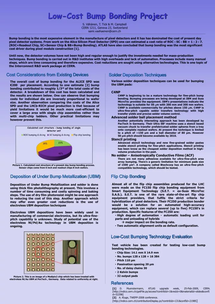
S. Vähänen, T. Tick & M. Campbell CERN 1211, Geneva 23, Switzerland sami.vaehaenen@cern.ch • Bump bonding is the most expensive element in the manufacture of pixel detectors and it has has dominated the cost of present day pixel detector systems. From work on the Alice Silicon Pixel Detector (SPD) one can estimated a cost ratio of ROC : SC : BB = 1 : 2 : 7. (ROC=Readout Chip, SC=Sensor Chip & BB=Bump Bonding). ATLAS have also concluded that bump bonding was the most significant cost driver during pixel module construction [1]. • Until now, the detector volumes have not been high and regular enough to justify the investments needed for mass-production techniques.Bump bonding is carried out in R&D institutes with high overheads and lack of automation. Processes include many manual steps, which are time consuming and therefore expensive. Cost reductions are sought using alternative technologies. This is one topic of the Interconnect R&D work package at CERN. Cost Considerations from Existing Devices Solder Deposition Techniques • Various solder deposition techniques can be used for bumping the UBM pads: • C4NP • C4NP is beginning to be a mature technology for fine-pitch bump bonding. Bumping processes are being developed at IBM and Suss MicroTec provides the equipment. IBM’s presentations indicate the technology is suitable for 50 mm with 200 mm and 300 mm wafers. C4NP is available commercially for pitches above 150 mm. C4NP is ultra-fine-pitch capable solder transfers technology with high transfer yields and precise solder volume control. • Advanced solder ball placement method • Another potentially interesting approach has been developed by PacTech in Germany. Their Ultra SB2 machine uses a stencil based vacuum chuck to transfer prefabricated solder spheres from a tray onto complete readout wafers. At present the technique is limited to a pitch of ~150 μm and a ball diameter of 80 μm. However 50 μm pitch should become available by 2010. • Stencil printing • Advanced stencil technology and new fine-grained solder pastes enable stencil printing for fine-pitch applications. Stencil printing has been know as the cheapest solder deposition method in high-volume production in the past. • No solder – Anisotropically Conductive Films (ACF) • There are not many adhesives available for ultra-fine-pitch area array bumping. There’s a generic limitation for minimum pads size of 1500 μm2. A company called Btechcorp has an ultra-fine-pitch compatible technology, which should be tested. The overall cost of bump bonding for the ALICE SPD was €200 per placement. According to one estimate [2] bump bonding contributed to roughly 1/3rd of the total costs of the detector. A breakdown of this cost has been calculated and the results are shown below. One can observe that bumping costs for individual die are inversely proportional to wafer size. Another observation comparing the costs of the Alice SPD and the LHCb-RICH pixel production is that because of yield limitations it would be much more cost-efficient to cover a large area with single chip assemblies rather than with multi-chip ladders. Other practical limitations may however prevent this. Low-Cost Bump Bonding Project Picture 1. Calculated cost structure of a present day bump bonding process. Sensor chips come from 6 inch and readout chips 8 inch wafers. Deposition of Under Bump Metallization (UBM) Flip Chip Bonding • Almost all of the flip chip assemblies produced for the LHC were made on the FC150 flip chip bonding equipment from Smart Equipment Technology (S.E.T. = ex-SussMicroTec S.A.S.). S.E.T. is one of the rare state-of-the-art flip chip equipment providers, that fulfils the strict criteria for hybridization of pixel detectors. Their FC250 production bonder would be a solution for an automated high-accuracy equipment, which can replace several (up to five) FC150’s in production. Specific features of the FC250 are: • High degree of automation - automatic loading unit for parts and unloading of hybrids • major impact on the bonding rate. • Two automatic alignment units as default configuration. • Deposition of Under Bump Metallization and solder is done using thick film photolithography at present. This involves a number of time consuming and costly spinning and baking steps. The use of dry film photoresist might be one approach to reducing the cost of this step. Another approach which may offer even greater cost reductions is the use of electroless UBM deposition techniques • Electroless UBM depositions have been widely used in manufacturing of commercial electronics, but its ultra-fine-pitch capability is unknown. Study of potential use of the electroless Ni/Pd/Au technology in UBM deposition is ongoing. Low-Cost Bumping Technology Evaluation • Test vehicle has been created for testing low-cost bump bonding technologies. • Chip Size: 14.1 mm X 14.9 mm • No. bumps 128 x 128 = 16 384 • Pitch 110 µm • Passivation opening 20 µm • No. of daisy chains 30 • 2 Kelvin bumps • 32 output pads Picture 2. This is an image of a Medipix2 chip which has been treated with electroless Ni/Au UBM at PacTech , Germany. Data related to uniformity at right. References [1] D. Muenstermann, ATLAS upgrade week, 25-Feb-2009, CERN. [http://indico.cern.ch/getFile.py/access?contribId=1&resId=0&materialId=slides&confId=52298] [2] A. Kluge, TWEPP-2008 conference. [http://indico.cern.ch/contributionDisplay.py?contribId=131&confId=21985]