Download
1 / 33
330 likes | 504 Views
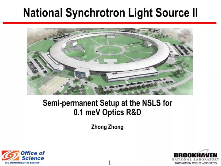
National Synchrotron Light Source II. Semi-permanent Setup at the NSLS for 0.1 meV Optics R&D Zhong Zhong. Acknowledgement. Collaborators: Lonny Berman, Yong Cai, John Hill, Xianrong Huang, Yuri Shvyd’ko, and Peter Siddons Technical help:

E N D
National Synchrotron Light Source II Semi-permanent Setup at the NSLS for 0.1 meV Optics R&D Zhong Zhong
Acknowledgement Collaborators: Lonny Berman, Yong Cai, John Hill, Xianrong Huang, Yuri Shvyd’ko, and Peter Siddons Technical help: Scott Coburn, Shu Cheung, Richard Greene, Anthony Lenhard, Zhijian Yin, and Hui Zhong Expert advice: Alfred Baron, Michael Hart, Steve Hulbert, Chi-Chang Kao, and Francesco Sette, and many others
Why Bother? • A semi-permanent setup is attractive for serious experimentalists • 0.1 meV R&D will involve lots of trial-and-error … a local home base is preferred • Access may entice experts (such as Shvyd’ko, Alp, Baron) to come to BNL more often • A playground may entice local experts (Siddons, Berman, Kao to name a few) to roll up their sleeves, and play • Develops local expertise: one can only learn by doing, and making mistakes • Readily available x-ray is a NSLS-advantage, a luxury for APS, ESRF and Spring-8
The Approach • 0th-order approximation: Repeat the Shvyd’ko experiment (0.7 meV target) • Get to the end results as soon as we can, then work backwards • Small crystals will be used • It may be advantageous to have a CCD detector to watch the beam from day-one. The detector helps in understanding what really goes on in the crystals • Study and refine: surface quality? Crystal d-spacing uniformity? Crystal strain/mounting? Temperature uniformity and stability? Role of dispersion compensation? … • The list goes on, but the point is to get our hands dirty and start learning. • We hope to migrate/creep/leap: 0.7 meV -> 0.3 meV -> 0.1 meV
Feasibility • Involves direct beam, flux should not be a problem. • The angles involved are large (a few to 100 micro-radians) -> Vibration should not be a problem. • The divergence Shvyd’ko used is 15 micro-radians. We can do that at the NSLS with 200-micron slit at 15 m. • 200 micron in-plane -> 4 mm footprint on C, W crystals (b=20), and 4/tan(1.5)=120 mm on D crystal (1.5 deg offcut). Thus small crystals are sufficient. • Temperature stability is important but we can start with ambient and see what other problems we have.
Haves and Have-nots • What we have: • Access to X12A: NSLS R&D beamline on a bending magnet port • Control system, 111 channel cut monochromator • A CCD detector borrowed from X15A (10 micron pixel size, 30 x 40 mm2) • What we made: • Two asymmetric (88.5 deg) 008 D crystals • Two 220 CW crystals, with fancy 200-500 micron thin wafer • … Enough to keep us going for a while • What we (eventually) need • Temperature controlled crystal environment • Scanning diagnostic aperture in beam • A dedicated high resolution detector
CW (Collimator and Wavelength Selector) Crystal APS Design W C
NSLSII CW Channel-Cut Design lap 1.5 3/4 W 200-500 microns 3/8 3/8 400 2-20 1 C 19 deg 26 deg Weak link side-view 1/8 -2-20 040 Quantity: 2, cut 1.5x1x2, polish top, cut channels, slice into 2 crystals 004 W C 1 top-view
CW Tilt and W Tweak W 220 leaf spring, ½ mm thick 9.1315 keV C tth=41.4 deg, th=20.7 Tweak Epoxy Ball-bearing 2 picomotors 1.7 deg Tilt Newport tilt #39 http://www.newport.com/store/genproduct.aspx?id=144557&lang=1033&Section=Graphics
D Crystal (Dispersion Element) APS Design
NSLSII D Crystal Design 4 Top surface polished 1 400 1/8 400, 1.5 degrees offcut end- view 1/4 3/8 004 side-view 004 lattice planes 3/8 T shape to minimize weight and maximize stiffness 040 top-view 1 Quantity: 2, cut 4x2x3/8, polish top, slice into 2 crystals
Cutting from a 5-inch 004 boule 4 400 400, 1.5 degrees offcut 004 side-view 004 lattice planes 3/8 Radial cutting to minimize longitudinal d-spacing variation during crystal growth
Rough Cutting at the BNL Central Shop Abrasive Water Jet
CW Crystal NSLSII CW Crystal Before etching 0.4 mm 1 mm After etching Two blanks for future
Assembled in Beam 0.5 mm 1 mm After etching Two blanks for future Tilt Tweak
C Crystal Rocking Curve W C • Data is for 0.3x12 mm and 0.3x1 mm beams • Width (FWHM) is about 120 micro-radians, in agreement with expectations of 106 micro-radians • Monochromator energy was changed, and dE/E=dth/th was used to calibrate tilt motor
Beam Off CW Image plate 50 micron resolution Tuned By-passing W W Half-tuned 1 mm C Through W Detuned ¼ -tuned Imperfections mostly due to coating on Be window 12-mm wide
Rocking Curves Through W tuned ½ detuned C rocking curve, through tuned W W Rocking curve
W Transmissivity • Experiment w/ 0.2x1 mm beam • Simulation assumes 0.35 mm thick W • Excellent qualitative agreement • Peak Transmissivity is about 40%, in agreement with simulation of about 45%. • Measurement is consistent with 80% W intrinsic transmissivity.
NSLSII D crystal Glued Epoxy RTV Spare Leveling pin, removed later
Poor-person’s Temp. Stabilization • Lights were turned off, and hutch door was closed overnight • Everything else stayed the same Before After 20 min. scan time
What Next? • Further characterization of D crystal • Verify the angular acceptance by mis-aligning the CDW assembly. • Design and build a second set of CDW assembly • CDW will be scanned against the second set to determine the energy resolution. • Depending on the resolution achieved, 0.3 or 0.1 meV version will be designed and tested.
Summary • NSLS bending magnet is suitable for 0.1 meV R&D. • CW Crystal performs as expected. Two such crystals in hand will be used for further development • Vibration control is appropriate (keeping it simple and stiff, minimize adjustments/weak links). • Free-standing thin-wafer concept provides good strain-relief for W crystal • Leaf-spring/weak-link mechanism provides fine adjustment
C Rocking Curve Simulation 111 pre-mono 220 intrinsic Convolved
CW Dumond Diagram < 5 micro-radians Beam through W