Download
1 / 25
250 likes | 385 Views
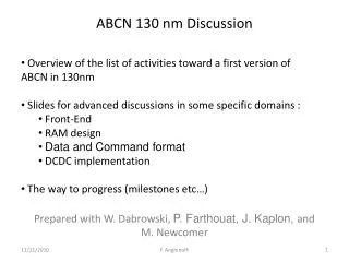
130 nm Stave Module Status. Slides from many sources ABC130 Issues/Investigation Module Design DC-DC converter work Plans/schedule after ABC130 Issues. ABC130 Early Tests and Findings. After lot of trials there was no DATA sent out of the ABC130 when instructing a register read

E N D
130 nm Stave Module Status Slides from many sources ABC130 Issues/Investigation Module Design DC-DC converter work Plans/schedule after ABC130 Issues
ABC130 Early Tests and Findings • After lot of trials there was no DATA sent out of the ABC130 when instructing a register read • Registers write where known to work (DAC controls, Voltage Regulator controls) • Clocks were known to be distributed in chip (thanks to the Scan Chain I/O) • Reset was known to be OK • Power was in range of what was expected FA
Early Tests and Findings • After inspection the problem was traced back to the control of the directions of the DATA and XOFF I/Os The same control bit (“dir”) controls the state of the core interface to XOFF/DATA and the driver or receiver state of XOFF and DATA (shown here when dir=0) Sending Data Not listening CORE LOGIC Sending Data Not listening Sending 0 Listening Sending 0 Listening “0” “0” “0” “0” R D I O R I O D I O I O XOFFL DATAL DATAR XOFFR Luckily can be fixed by changing only one metal layer FA
FIB Done in UK A B B cut • Can “repair” with focused ion beam (FIB), but not cheap, k£’s each • Because of expensive costs, firstfew chips (3) were processed only on the “right” corner • Fixing one corner is enough to see DATA and evaluate all the chip features except the DATA and XOFF passing mechanism • 5 more were fixed in both corners • Fixing two corners should allow to fix unidirectional DATA and XOFF passing (so 2 versions are needed to validate left or right) A XOFFR DATR add DATR FA FA 03/02/14 4
ABC130 Preliminary Results (2) PRELIMINARY 1 sensor ~0.8pF unbonded 2 sensors ~1.6pF Preliminary noise data at 150V bias ABC130 with two ATLAS07 mini sensors Noise is as expected. To date - apart from the known “feature” - ABC130 is working well. ACES, CERN, 19/04/2014
ABC130 Preliminary Results (1) • Evaluation of single FIB die continues • Test PCB • Probe Card • Test coverage to date: • Register write/read • DACs & LDOs • 40, 80, 160 MHz DCLK • Noise with mini sensors • Mean Power vs trigger rate • Pending • Clock margin (higher BCO) • Power vs time • Gain calibration • beam, laser, source… • SEU studies • Irradiation • … ABC130 under Probe Test ABC130 DAC & LDO Characteristics ACES, CERN, 19/04/2014
FIB Hybrid • Used as test vehicle to evaluate multiple ABC130s being readout • Part of ongoing evaluation of ABC130 asics • Checks data passing between multiple devices • Coherent affects due to multiple devices being powered, clocked and triggered • Ultimate goal is to hook up to an ATLAS large area sensor • Check noise performance and stability Chip IDs 9 8 Chips 5:9 are FIB’d versions 7 • Circuit comes as a thin build FR4 • 3 layers of ~350µm build thickness • Trying to emulate flex circuit build... • Slightly oversize in length for handling • Will overhang sensor • Circuit will come with 10 ascis attached • 5 off FIB’d and 5 off non-FIB’d • Due to cost of FIB’dasics • All 10 chips linked serially (for data readout) • Only 5 FIB’d chips can ever be readout • These devices have dedicated data paths as well • Backup in case serial readout doesn’t work • Should still be able to configure ALL chips • Used to test power consumption etc. The reality 6 5 4 3 2 1 0
FIB Module Test Frame Pin1 Serial Power Monitor – leave open circuit Samtec connection to ABC130 Driver Board Sensor HV filter NTC monitor HV HVRet Power Return DCDC Power In DCDC Plugin (rotated 180° compared to CERN type)
FIB Hybrid - Status • 5 FIB’d chips probed. All working. • 1 Hybrid with 5 FIB’d and 5 non-FIB’d ASICs glued and bonded • Power and on-chip termination as expected • Can see regulation to 1.36 V with no init • Current is 600 mA for 10 ASICs • Termination 30 ohm with 3 chips’ termination enabled • Plan on checking signal quality versus termination • 1 Hybrids went go down to RAL with Ash and Sam Monday • First hybrid with 10 off non-FIB’dasicsglued to sensor Tuesday • Allows to check if gluing/bonding affects sensors • Allows for checking of bonding parameters • Hopefully FIB’d ASIC hybrid will be glued into module Thursday • Allows for a week of testing with increasing FE bonded • If all goes well, might be able to check on-detector DC-DC before AUW • Upon successful testing of hybrid at RAL bring back both circuits to Liverpool FIB’d ASIC
ABC130 Resubmission • So far, everything but gain and noise as expected • Good enough to use • Changes to metal layer complete • If tests go well, should have all the results to start the re-spin at AUW • Will take roughly 4 months to receive wafers after submission • Implies ~Sept-Oct for first ASIC • Will probe ASICs so first module should be available in beginning of new year (roughly 1 year delay)
ABC130 Barrel Module • Module is made up of 3 main parts: • Sensor • Flex circuits (carrier for readout asics and I/O buffer) • Power Board (SPP or PoL DC-DC) with sensor filtering • Moving towards an integrated module • Flex circuits and powering attached within sensor area • Sensor provides mechanical support and thermal management Module Power and Sensor Bias Power Board 10cm x 10cm Sensor Hybrid (10 x ABC130 and 1 x HCC) Hybrid (10 x ABC130 and 1 x HCC) TTC and Module Data 16.5mm 8mm 16.5mm Thermo-Mechanical Module with Prototype DCDC converter
Integrated Powering using a toroidal based DCDC converter • Power board to be located between the 2 hybrids • Functionally to be identical to current converters • Use identical buck regulator • 1-wire controllable • Plus sensor HV filtering added • Geometry set by • Gap between hybrids, comes in at ≤10mm • “No go” area for pick up tool when placing module onto stave • Assume 5mm suction cup central to sensor • Sets board form factor to ~44mm x 8mm Power Board 48.77mm No Go • Board dimensions 43.75mm x 8mm • Board dimensions show minor increase (from predicted) • Due to use of a larger 1-wire device (due to availability) • Addition of shield box clips • 4 layer build using 35µm Cu, build thickness ≤0.8mm • 3 active layers and 1 shield layer • Comes in PCB frame with connector for testability • As per CERN STV10 converters • Can be detached when required for module mounting • Shield box – chemically etched Aluminium • Attached using clips (sets metal thickness ~100µm) • Target height ~7mm • Layout finished and ready to go for manufacture 10mm Al Shield Box (Photofabrication) Prototype toroidal coil
Toroidal based converter - detail Filtered HV to sensor Power In and control HV filtering block • PCB layout based on guidelines presented at TWEPP10 • (C.Fuentes et al: Study and methodology for decreasing noise emissions of • DC-DC converters through PCB layout) • Some minor changes to component sizing due to geometrical constraints • Results in increased component package inductance (and noise?) • Sensor HV filtering block adheres to 500V clearance specification • Exposed conductors >1.75mm clearance • Comes with NTC (accessible via bond pads) • Provides temperature interlock during module testing • 1-wire control would be replaced with HV switch and controls in final modules • Size depends on switch-yet to be found Raw HV from both hybrids 1-wire control DCDC out to both hybrids NTC DCDC Power Block 24mm 8mm Courtesy of Sam Powell
Serial Power Board and SPP • Take existing Toroidal based DCDC converter board • Bond pads to/from bus tape and hybrids are fixed by this • Remove DCDC converter circuit and 1-wire whilst retaining Sensor HV filtering • Should now be able to define the form-factor for the SPP board SPP 2mm x 2mm (drawn to scale) 18.5mm (20+mm?) Might still have to extend the length to accommodate a small number of 1206/0805 smds (2 off?) 43.75mm 8mm • Prototype SPP ASIC (University of Pennsylvania) • 2mm x 2mm asic (with 4 x SMDs) • Provides Serial Power Protection and control • 1-wire controller, as used for DCDC, is no longer required • Use this free space for SPP • Provisional board form factor shown above • Significant reduction in real estate compared to Toroidal based DCDC converter • ~60% smaller • Also true for height – no shield box required DCDC circuit DCDC
Prototype DC-DC Converters • Converter Dimensions (L x W x H): 44 x 8 x 6.5 mm • 4 Layer build using 1oz Cu • Hand wound elliptical inductor (200nH/26mΩ) • Converter circuit based on CERN STV10 • With reduced sized SMDs (0805 instead of 1210) • Plus 1-wire control and HV filtering ABC130 Prototype Converter Leakage from shield box (~15e increase) Test on ABCN-25 module Input Noise: 600e (598e) Planar Coil Prototype Converter Input Noise: 602e (604e) Reference measurement shown in brackets (CERN SM01C converter) Test on ABCN-25 module Converter placed <3mm from bond wires • Involves embedding coil within PCB • Significant reduction in height compared to toroidal coil • Target height <4mm with shield • Making integration and cooling of coil easier • Based on commercial LTC3605 buck regulator • As per CERN type • Wrap-around shield added to encompass noisy circuitry • Efficiency comes in at 77% at 3A Input Noise: 616e (598e) Input Noise: 625e (604e)
Converter at 4MHz • Switching frequency of Buck regulator increased from 2MHz to 4MHz • Should allow smaller sized components to be used, making integration/packaging easier • Inductor now ~110nH (was originally ~220nH) and DC resistance now ~14mΩ (was ~26mΩ) • Target 5 mm height using commercial solenoids- shown toroids not needed • Tests done with converter on sensor, largest sized component is 0805 • Input noise is more or less identical to previous measurements using ~200nH coil at 2MHz • Efficiency is coming in at ~77% at 2A (predicted ABC130 module current consumption) • Was originally 70-72% operating at 2MHz Input Noise: 603e (600e) Input Noise: 606e (602e) Value in brackets is original noise measurement at 2MHz using 0805 components DTN at 0.4fC Only see evidence of converter at 0.4fC, all other threshold settings show approx zero occupancy
Plans for TM and electrical modules (1) EoS Side IO • Extra ABC130 investigation has caused delays all over WP3 • HCC submission delays until May. Delivery Oct/Nov • As HCC not “final”, still can’t submit electrical hybrids SLVS to ABC130 SLVS to ABC130 4.70mm Bidirectional SLVS to ABC130 Bidirectional SLVS to ABC130 Bidirectional SLVS to ABC130 Bidirectional SLVS to ABC130 2.86mm IBM CMOS 8RF
Plans for TM and electrical modules (2) • Extra mechanical/bonding trials needs for FIB’d hybrid/module delayed progress finalizing tooling changes needed for hybrid-to-sensor gluing (glue stencil development and pickup changes) • Delays TH module program start in Liverpool • Metrology and assembly of completed components for jigs sets for Cambridge, B’ham, Glasgow, LBL, UCSC also delayed as manpower all focused on FIB’d prototypes • Delays TM module program start everywhere else ACES, CERN, 19/04/2014
Some good news • Circuits designed for Stave Thermal studies and Hybrid/Module tooling evaluation • Converged to single flavour tab across ALL hybrids • Using flexible resist • 80 circuits went out early January (10 off panels) • Arrived and look excellent. Flexible resist
Summary of WP3 effects on WP4 • TM module program delayed until May/June to make first components at Liverpool • Would expect enough for first stave in Q3 2014 • Electrical modules delayed until Dec 2014/Jan 2015 as will be receiving HCC and ABC130 re-spin at same time. • This pushes first stave back to Q3/2015 and powering decision into 2016.
Backup stuff ACES, CERN, 19/04/2014
Chip Pickup Tool Fix Plastic Bar Epolite Chip Pickup Tool Hybrid Sensor Bar would locate in the two dowel holes and the additional slot • We want to put a removable bars on chip pickup tool to push on outside of hybrid • Under design and prototyping now • Will add a groove into chip pickup tool to locate and hold bar • Needs to avoid HCC region for both types of hybrids Slide 24
Assembly Future Plans (I) Stencil would be for one hybrid (this shows paper stencil onto sensor for two hybrids • Once pickup tool bar shown to stabilize unsupported hybrid will make metal stencil to screen Epolite onto back of hybrid • Without bar, epoxy will pump between stencil and hybrid, binding hybrid to it. Slide 25