Download
1 / 39
390 likes | 540 Views
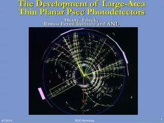
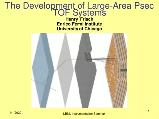
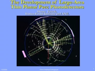
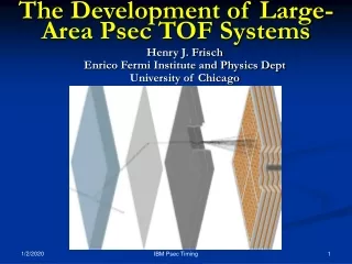
The Development of Large-Area Thin Planar Psec Photodetectors. Henry Frisch, Enrico Fermi Institute and ANL . The Large-Area Psec Photo-detector Collaboration.

E N D
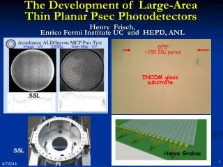
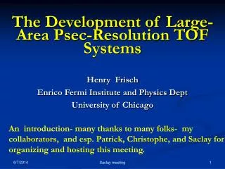
The Development of Large-Area Thin Planar PsecPhotodetectors Henry Frisch, Enrico Fermi Institute and ANL Fermilab Detector Workshop
The Large-Area Psec Photo-detector Collaboration 3 National Labs, 6 Divisions at Argonne, 3 US small companies; electronics expertise at UC Berkely, and the Universities of Chicago and Hawaii Goal of 3-year R&D- commercializable modules. DOE Funded (a little NSF)
Three Goals of a New (1 yr-old) Collaborative Effort: • Large-Area Low-Cost Photodetectors with good correlated time and space resolution (target 10 $/sq-in incremental areal cost) • Large-Area TOF particle/photon detectors with psec time resolution ( < 1psec at 100 p.e.) • Understanding photocathodes so that we can reliably make high QE, tailor the spectral response, and develop new materials and geometries (QE > 50%?, public formula) Fermilab Detector Workshop
Detector Development- 3 Prongs MCP development- use modern fabrication processes to control emissivities, resistivities, out-gassing Use Atomic Layer Deposition for emissive material (amplification) on cheap inert substrates (glass capillary arrays, AAO). Scalable to large sizes; economical; pure – i.e. chemically robust and (it seems- see below) stable Readout: Use transmission lines and modern chip technologies for high speed cheap low-power high-density readout. Anode is a 50-ohm stripline. Scalable up to many feet in length ; readout 2 ends; CMOS sampling onto capacitors- fast, cheap, low-power (New idea- make MCP-PMT tiles on single PC-card readout- see below) Use computational advances -simulation as basis for design Modern computing tools allow simulation at level of basic processes- validate with data. Use for `rational design’ (Klaus Attenkofer’s phrase). Fermilab Detector Workshop
4 Groups + Integration and Management HJF: LAPPD Advanced Photo-Detector Status
PET (UC/BSD, UCB, Lyon) Collider (UC, ANL,Saclay. Mass Spec Security (TBD) DUSEL (Matt, Mayly, Bob, John, ..) K->pnn (UC(?)) Parallel Efforts on Specific Applications Explicit strategy for staying on task . LAPD Detector Development Muon Cooling Muons,Inc (SBIR) ANL,Arradiance,Chicago,Fermilab, Hawaii,Muons,Inc,SLAC,SSL/UCB, Synkera, U. Wash. Drawing Not To Scale (!) All these need work- naturally tend to lag the reality of the detector development Fermilab Detector Workshop
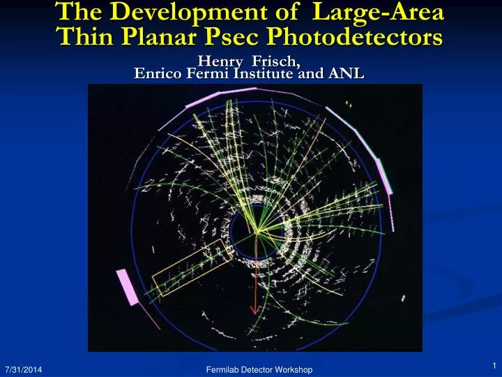
At colliders we measure the 3-momenta of hadrons, but can’t follow the flavor-flow of quarks,the primaryobjects that are colliding. 2-orders-of-magnitude in time resolution would all us to measure ALL the information=>greatly enhanced discovery potential. Application 1-Colliders A real top candidate event from CDF- has top, antitop, each decaying into a W-boson and a b or antib. Goal- identify the quarks that make the jets. (explain why…) Specs: Signal: 50-10,000 photons Space resolution: 1 mm Time resolution 1 psec Cost: <100K$/m2: t-tbar -> W+bW-bbar-> e+ nu+c+sbar+b+bbar Fermilab Detector Workshop
Application 2- Neutrino Physics • Spec: signal single photon, 100 ps time, 1 cm space, low cost/m2 (5-10K$/m2)* (Howard Nicholson) Fermilab Detector Workshop
Application 3- Medical Imaging (PET) Alternating radiator and cheap 30-50 psec planar mcp-pmt’s on each side Can we solve the depth-of-interaction problem and also use cheaper faster radiators? Depth in crystal by time-difference Simulations by Heejong Kim (Chicago) Heejong Kim Heejong Kim Depth in crystal by energy- asymmetry Fermilab Detector Workshop
Application 4- Cherenkov-sensitive Sampling Calorimeters A picture of an em shower in a cloud-chamber with ½” Pb plates (Rossi, p215- from CY Chao) Idea: planes on one side read both Cherenkov and scintillation light- on other only scintillation. • I A `cartoon’ of a fixed target geometry such as for JPARC’s KL-> pizero nunubar (at UC, Yao Wah) or LHCb Fermilab Detector Workshop
The 24”x16” `SuperModule Fermilab Detector Workshop
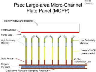
Sealed Tube (Tile) Construction • All (cheap) glass • Anode is silk-screened • No pins, penetrations • No internal connections • Anode determines locations (i.e. no mech tolerancing for position resolution) • Fastens with double-sticky to readout Tray: so can tile different length strings, areas • Tile Factory in works (ANL) Fermilab Detector Workshop
ANL-UC Glass Hermetic Packaging Group • Proceed in 3 steps: 1) hermetic box; 2) Add MCP’s, readout, (Au cathode); 3) Add photocathode Box Box+ 8” MCPs Possible Au anode Box+MCP+PC Yr 3 Yr 2 Yr 1 Fermilab Detector Workshop
SSL Photocathode Process Chamber OssySiegmund, Jason McPhate, Sharon Jalinsky UV Transmissive Window Glass Window Manipulators 18” ID Chamber UHV valves Photo-Cathode Forming Well Flange 16.5” Detector Loading Flange Ion Pump supply Ion Pumps Fermilab Detector Workshop 14
SSL Photocathodes: Processing Oven, Cathode Deposition • Oven accommodates Large Format Inside Envelope: 36” x 30” x 25” High • Defines Large Chamber Limits • Cathode station controls alkali metal deposition, and monitors cathode response Ossy Siegmund HJF: LAPPD Advanced Photo-Detector Status • 15
Advanced Photocathode Group Moving to understanding the physics • III-V have the potential for high QE, shifting toward the blue, and robustness i.e. they age well, high-temp) • Opaque PC’s have much higher QE than transmission PC’s- we have the geometry • Many small factors to be gained in absorption, anti-reflection- see papers by Townsend and talk by Fontaine on our web site • Quantum Effic. Of 60% have been achieved in bialkalis Klaus Attenkofer, Sasha Paramonov, Zikri Yusof, Junqi Xi, Seon Wu Lee, UIUC, WashU, …. Big payoff if we can get >50% QE robust Photocathodes, and/or more robust (assembly). Also want to get away from `cooking recipes’ to rational design. Fermilab Detector Workshop
MCP/Photocathode Development- Test setup at APS laser Bernhard Adams, Klaus Attenkofer, (APS), Matt Wetstein (HEP) HJF: LAPPD Advanced Photo-Detector Status
Characterization of Materials • Igor Veryovkin, Slade Jokela, Thomas Proslier, Alexander Zinovev (MSD)- joint meeting with ALD and Photocathode groups, also works closely with simulation • Have constructed dedicated setup for low-energy SEE and PE measurements of ALD materials- parts on order. • Group also has parts-per-trillion capability for characterizing photocathodes after exposure to Argon, MCP’s before&after scrubbing, aging.
Simulation (crosses all groups)Valentin Ivanov, Zeke Insepov, Zeke Yusof, Sergey Antipov • 10μm pore • 40μm spacing • Funnel (!) • Large Area Photodetector Development Collaboration HJF: LAPPD Advanced Photo-Detector Status • 19
New Femtosec Laser Lab at APS • Bernhard Adams, Matthieu Chabon, Matt Wetstein Fermilab Detector Workshop
Electronics GroupJ.F. Genat, Gary VarnerHerve Grabas, Eric Oberla, Larry Ruckman, Kurtis Nishimura • text HJF: LAPPD Advanced Photo-Detector Status
PSEC-2 ASIC • 130nm IBM 8RF Process • This chip 4 channels, 256 deep analog ring buffer • Sampling tested at 11 GS/sec • Each channel has its own ADC- 9 bits eff (?) • The ADCs on this chip didn’t work due to leakage (silly, didn’t simulate slow easy things) - resubmitted, and test card out for fab with external ADC - will use 1 of 4 chnls • We’re learning from Breton, Delagnes, Ritt and Varner (Gary is of course a collaborator) Fermilab Detector Workshop
History- Key Ingredients • Seed Money Opportunities(pre big DOE proposal) • Seed Money From the PSD Dean • Competitive LDRD Program (3 yrs) • Competitive ANL-FNAL-UC Program • Competitive DOE ADR Program • French Consulate, Chicago-France Center (Comp) • Non-projectized good-will and friends, hubcaps… • Local (i.e. University) Technical Infrastructure • EFI Electronics Shop • PSD Engineering Center, Central Shop • UC undergrads, 1st yr grads, IMSA • SSL (UCB) – Anton, Ossy advice
History- Key Ingredients- cont. 3. Access to Lab Resources • Fermilab technical help- Greg Sellberg, SciDet • ANL SULI student (Camden) + Laser Lab (LDRD) Fermilab Test Beam- Erik, MTEST, PREP, safety,… 2. Post DOE Proposal – Key Ingrednts 1. Enlightened and visionary DOE Support (multi-level) • Portfolio of risk- willing to go for some high-payoff hi-risk projects in the portfolio (global competition) • Involvement with direction, scope, vision • Got us past the `start small, low-risk’ gap of death by reviewer – some things need to start big to succeed.
Post-prop Key Ingredients- continued 4. Enlightened Lab Management • Openness to crossing `silos’, new ideas, cross-disciplinary synergies (hard to do if `projectized’) • Willingness to change management structures to enable new alignments, needs • Direct involvement with universities, physics, young ones, staff, at all levels • Very low or no barriers to access to resources Fermilab Detector Workshop
Bottom Line- What does it take to have an Effective Univ.-Lab Project • A clear goal with near-term applications (e.g. 3-5yr) • Local infrastructure (engineers, machinists, computation) at the universities • Encouragement and seed funds at the university • Competitive opportunities like DOE-ADR, LDRD, FAACTS , SBIR for next level seeding • Risk portfolio management at the agencies for the next step after ADR, LDRD • Strong support, `moral and financial’, but also intellectual, from the Lab management • Access to talent at the Labs • Access to facilities at the Labs Fermilab Detector Workshop
More Information: • Main Page: http://psec.uchicago.edu • Library: Image Library, Document Library, Year-1 Summary Report, Links to MCP, Photocathode, Materials Literature, etc.; • Blog: Our log-book- open to all (say yes to certificate Cerberus, etc.)- can keep track of us (at least several companies do); • Wish us well- goal is in 3 years (2 from now) to have commercializable modules- too late for the 1st round of LBNE, but maybe not too late for a 2nd or 3rd-generation detector. Fermilab Detector Workshop
THE ENDThanks to everybody in the LAPPD collaboration who contributed to our progress, esp. the young ones. HJF: LAPPD Advanced Photo-Detector Status
The End- Fermilab Detector Workshop
Some Neutrino-specific Thoughts AREA Fermilab Detector Workshop Tiles are very robust against pressure – less risk of implosion, can build higher; Tiles have very small internal volume (0.6mm thick internally, close to half of that MCP capillary plate)- no shock? Can add area incrementally as transmission lines probably work well at 6 feet (8 tiles) => incremental cost is only the tile Tesselation is flexible- can have 8” by 72”, 16” by 24” (SM), optimized for app...
Some Neutrino-specific Thoughts DETECTOR DESIGN Fermilab Detector Workshop Spatial Res of <1cm plus 100% (well,.. ykwim) coverage would allow working close to the walls => greater Fid/Tot ratio; Also would make curve of Fid/Tot flatter wrt to symmetry- could make a high, long, narrow (book-on-end) detector at smaller loss of F/T; Cavern height cheaper than width; robust tubes can stand more pressure Narrow may allow magnetic field (!)
Some Neutrino-specific Thoughts SIGNAL TO BACKGROUND Fermilab Detector Workshop 100 psec time resolution is 3cm space resolution ALONG photon direction in a perfect world; Transverse resolution on each photon should be sub-cm; Question- can one reconstruct tracks? Question- can one reconstruct vertices? Question- can one distinguish a pizero from an electron and 2 vertices from one? (4 tracks vs 1 too)
VERTEX RECONSTRUCTION (forgive my ignorance- fools rush in where angels fear to tread.) Fermilab Detector Workshop Question: Can we reconstruct the first 3 radiation lengths of an event with resolution ~1/10 of a radiation length? Handles on pizero-electron separation: 2 vs 1 vertices; no track vs 1 track between primary vertex and first photon conversion; 2 tracks (twice the photons) from the 2 conversion vertices; Know photon angle, lots of photons-phit Book-on-end aspect ratio helps against dispersion, scattering-have to look at whole picture.
New MCP Structure (not to scale) pore 1 KV • resistive coating (ALD) • emissive coating (ALD) • conductive coating (thermal evaporation or sputtering) Jeff Elam Fermilab Detector Workshop 34
Atomic Layer Deposition (ALD) Thin Film Coating Technology • Atomic level thickness control • Deposit nearly any material • Precise coatings on 3-D objects (JE) • Lots of possible materials => much room for higher performance Jeff Elam pictures Fermilab Detector Workshop
Put it all together- the `Frugal’ MCP • Put all ingredients together- flat glass case (think TV’s), capillary/ALD amplification, transmission line anodes, waveform sampling • Glass is cheap, and they make vacuum tubes out of it- why not MCP’s? Fermilab Detector Workshop
Put it all together- the `Frugal’ MCP • Put all ingredients together- flat glass case (think TV’s), capillary/ALD amplification, transmission line anodes, waveform sampling • Glass is cheap, and they make vacuum tubes out of it- why not MCP’s? Fermilab Detector Workshop
The 24”x16” `SuperModule • Tile now has no penetrations- neither HV nor signals • Digital card in design • Front-end ASICs ditto • Mockup of 2x3 SM • Real parts- but no MCP • Tile tests in ~3 months? Fermilab Detector Workshop
GodParent Review Panels • Electronics Group • Photocathode Group • MCP Group • Packaging Group • Karen Byrum • K.Arisaka • J. Elam • D. Ferenc • J.F. Genat • P. Hink • A. Ronzhin • Bob Wagner • K.Attenkofer • Bross • Z. Insepov • Tremsin • J. Va’vra • A. Zinovev • Gary Varner • J. Buckley • K. Harkay • V. Ivanov • Lyashenko • T. Prolier • M. Wetstein • Zikri Yusof • B. Adams • M. Demarteau • G. Drake • T. Liu • I. Veryovkin • S. Ross HJF: LAPPD Advanced Photo-Detector Status