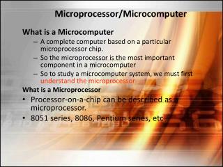
MICROPROCESSOR
MICROPROCESSOR. Yrd. Doç. Dr. Mehmet Ali Aktaş. Logic Gates And Their Uses. A gate is a simple electronic circuit that has a single output voltage that corresponds to one of the two binary values .

MICROPROCESSOR
E N D
Presentation Transcript
MICROPROCESSOR Yrd. Doç. Dr. Mehmet Ali Aktaş
LogicGates And Their Uses • A gate is a simple electronic circuit that has a single output voltage thatcorresponds to one of the two binary values. • Thesegatesareoftenreferred to as ‘logic gates’ and the output voltages as ‘logic 0’ or ‘logic1’ instead of binary 0 and 1. • Ifyouwere to ask a mathematician or a computer programmer, they willrefer to the outputs as binary values but an electronics engineer willcallthemlogiclevels.
LogicGates And Their Uses • We connect one or more voltages to the input of the gate. These inputvoltages are either logic 0 or logic 1 levels. The logic gate looks at theinput voltages and ‘decides’, depending on its design, what voltage toproduce at the output of the circuit. • There are only four basic designs of gate. They are called the NOT gate,the AND gate, the OR gate and the XOR gate.
LogicGates And Their Uses • It has only one input and performs a very simple function. It simplyreverses the binary value. If we put a logic 1, we get a logic 0 at theoutput. Similarly, a 0 at the input gives a 1 at the output. • A truthtable
LogicGates And Their Uses • Unlike the NOT gate, an AND gate has more than one input. In fact wecan have as many inputs as we like but the good news is that inmicroprocessors only two inputs are used. • An AND gate is any circuit that gives a logic (or binary) 1 if (andonly if) every input to the circuit is at logic 1. So in microprocessors,with only two inputs, it is easier to say that it gives a 1 out if both ofthe inputs is at logic 1.
LogicGates And Their Uses • What is the point of an AND gate? • We often meet an AND gate without realizing it. When we climb intoan elevator the door must be closed AND the floor button pressedbefore the motor will start. This is an AND gate in action. • Unless we appreciate that the hex numbers are really just groups ofones and zeros, it may seem odd to talk about putting numbersthrough AND gates. In figure, hex inputs of 37H and 5BH havebeenused, andgiving a result of13H. • AND GATE DOESNT ADD NUMBERS.
LogicGates And Their Uses • The NAND gate • TheNAND gate is just an AND gate followed by a NOT gate so all theoutputs shown in the AND truth table are just inverted by the NOTgate. • On a diagram, this combination is indicated by putting a small circleon the end of the symbol.
The OR gate • The OR gate gives alogic one at its output if either (or both) of the inputs is at a logicone. Just like the AND gate, the OR gate can have as many inputsas we wish but in a microprocessor, we only use two inputversions. Its symbols and truth table are shown in Figures
The NOR gate • This is just the same as the OR gate except for theNOT gate added to the output.
The XOR gate • This is called the Exclusive-OR gate, which isabbreviated to XOR or EOR.
Arethesenumbersthesame? • 1011 1001
Thetri-statebuffer • This looks like a logic gate but behaves more like a switch. We can see that it is quite simple having only an input, an outputand another connection called an ‘enable’. • When the buffer is switched on, anysignal applied to the input appears at the output and when it is switchedoff, the buffer is disconnected so that there is no output signal present. • So, why not just use a switch? • The problem with a switch is that, once closed, the input and outputare physically joined so that input and output circuits are connectedtogether. The buffer is a one-way device for signals so that the outputis isolated from the input to prevent any changes in the next circuitfrom interfering with the input circuits.
RegistersAndMemories • The logic gates that we met in the last chapter occur in their millionsin microprocessors and in the surrounding circuitry. They are to befound in all microprocessors from the oldest and simplest. • When logic gates are used in a microprocessor they are usuallygrouped together into circuits, called flip-flops, each one being able tostore a single binary digit.
RegistersAndMemories • A flip-floporbistable • A flip-flop or bistable is a circuit that can store a single binary bit –either 0 or 1. One useful characteristic of the flip-flop is that it can onlyhave an output of 0 or 1.
RegistersAndMemories • The purpose of the clock input is to tellthe flip-flop when to accept the new input level. • The sequence of the events is: • Apply the binary level to be stored. • Wait a short time (a few nanoseconds) until the voltage is properlyestablished. • Apply a signal to the clock input to tell the flip-flop to memorize thesignal present at the input.
RegistersAndMemories • Why do we have to wait? • When we apply a voltage to a length of wire, we would hope that thevoltagechanges as in Figure.Unfortunately,it takes a fewnanosecondstosettledown.
RegistersAndMemories • The rise of voltage travels along theconnecting wire and is reflected from the end causing another voltageto be reflected towards the input. This reflection is itself reflected andafter repeated reflections, the voltage slowly settles down to its newlevelas in Figure
RegistersAndMemories • And what about the clock signal? • This is just an input to tell the flip-flop that it is time to read the inputlevel. All microprocessor operations are carefully timed by clockpulses to ensure that the system operates in the correct sequence. • The clock signal is usually a positive-going voltage pulse. This pulsecan be used to switch two circuits at different times by designing onecircuit to respond to an increasing voltage and the other to use adecreasing voltage. If, for example, the pulse in Figure were to be10 ns wide then this could create the required delay for the voltage tosettle.
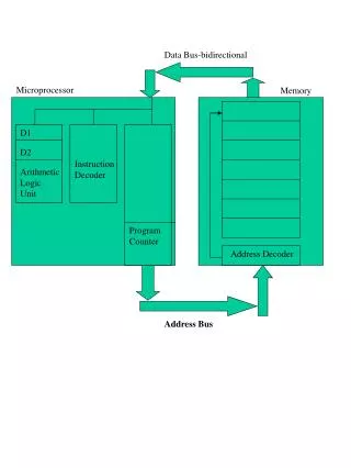
RegistersAndMemories • A register. • A register is just a collection of flip-flops. A flip-flop can only store onebit so to handle 32 bits at a time we would need 32 flip-flops andwould refer to this as a 32-bit register. To save space, Figure shows an 8-bit register.
RegistersAndMemories • The register has two distinct groups of connections: the data bits 0 to7 and the control signals. The data connections or data lines carry thebinary levels in or out of the register. The number of data linesdetermines the size of the register so a 64-bit register would have 64 data connections. • It may be interesting to look inside the register to see how the tristatebuffer is used to achieve this two-way traffic on a single wire.Have a look at Figure
RegistersAndMemories • Whatareregistersfor? • Registers are storage areas inside the microprocessor. Almost thewhole of the microprocessor is made of registers. They store the datathat is going to be used, they store the instructions that are to be usedand they store the results obtained.
RegistersAndMemories • In most cases, the data to be stored is applied to the inputs of theregister and, after a short pause to let the voltages stabilize, the registeris enabled by the voltage on the enable control. The information isthen safely stored until it is next required.Thesequence is: • The read/write line is taken to logic 0 to allow the register to receivedata from an external source. • The enable control switches ON the tri-state buffers at the input toeachflip-flop. • The data is written to each flip-flop and then the enable control putsthe register to sleep until the next time it is needed.
RegistersAndMemories • How long can it be stored? • It will be stored until the power supplies are removed – either by anequipment fault or, more usually, by the system being switched off.The data does not deteriorate in storage.
RegistersAndMemories • Shiftregisters • These are a variation on the register theme. They still consist of groupof flip-flops but the interconnections have been changed. Have a lookat the arrangement in Figure and see if you can guess the likelyoutcome.
RegistersAndMemories • This is called a shift register because the data is shifted from one flipflopto the next each time the clock pulse occurs. Specifically, the oneshown is a shift left register because each bit moves one place to theleft on each clock pulse. All the bits move at the same time. The lastone in bit 7 drops off the end and is lost while at the other end, a newbit is entered into bit 0.3610
RegistersAndMemories • Follow the sequence through and in particular note what happens tothenumbersstored: • After one clock pulse, all the bits will have moved one place to theleft. A new ‘0’ will have entered bit 0 and the last, which was in bit7, will have fallen off the end of the world. The bits stored at thistime are 01001000 and the numerical value is 48H or, in denary,7210. Notice how shifting the bits to the left has multiplied the valueby2. • After eight clock pulses, all the existing data in the register will havebeen flushed out and refilled with zeros. The register will hold thenumber zero so there is a limit to how many times we can multiplybyshiftingtheregister. • After 5000 clock pulses, it is still full of zeros. Admittedly, they willbe new zeros that have replaced the others but that will not makeanydifference.
RegistersAndMemories • By re-arranging the register, it is easy to produce a shift-right register asin Figure This has all the same properties except it shifts datatowards the right and divides the number by two each time the clockpulseis entered.
RegistersAndMemories • One example would be automatic checking of inputs. In Figure it is controlling an automatic ticket dispenser. The customer insertssome money and presses any button of the eight available to obtain theticket required – but which button was pressed?
RegistersAndMemories • As a button is pressed the voltage output can be designed to changefrom logic 0 to logic 1 so to start with, we can assume no buttons arepressed and the response from each button is zero. Along comes acustomer who, having read the instructions, inserted some money andre-read the instructions and stared at the buttons, eventually decides topressa button. • Pressing a button generates a burst of eight clock pulses and the valueof each button is loaded into the shift register. Once the button hasbeen pressed the zeros and ones corresponding to each of the buttonsis loaded into the shift register. The output from each button is madeavailable to external circuits and one such circuit will be activated anda ticket will drop down the chute
RegistersAndMemories • For how long would the customer have to press the button? • The microprocessor is amazingly fast compared with us. • Most people would therefore press a button for at least 0.1 s. So whatcan the microprocessor do in the same 0.1 s? A modern microprocessorcan check a button in about 0.25 μs or 0.25 millionths of asecond. In other words, it can check about 4 000 000 buttons in asecond.
RegistersAndMemories • Rotateregisters
RegistersAndMemories • Memories (NEXT LECTURE)