Microprocessor
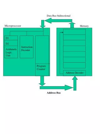
Microprocessor. The Architecture of a µP. Registers. R1. R2. Arithmetic Logic Unit (ALU). Control Circuitry (CU). R3. R4. …. Rn. Bus. I/O for external Communication. Registers. Temporary storage unit within the CPU Some registers have dedicated uses


Microprocessor
E N D
Presentation Transcript
The Architecture of a µP Registers R1 R2 Arithmetic Logic Unit (ALU) Control Circuitry (CU) R3 R4 … Rn Bus I/O for external Communication
Registers • Temporary storage unit within the CPU • Some registers have dedicated uses • Others are for more general purpose use • Often in some µP one register is specially known as Accumulator • Numbers of registers vary from µP to µP
Operation of µP 2. Decode 1. Fetch 3. Execute
8086INTRODUCTION Intel Datasheet Rafiq 3.1 Hall Brey
8086 Features First 16 bit processor from Intel introduced in 1978 produced from 1978 to 1990s CPU clock speed 5MHz to 10MHz Packaged in 40-pin DIP 8 general purpose register prefetches up to 6 instructions from memory and queues them within the chip to speed up execution
8086 Features... 16 bit data bus 20 bit address bus can address up to 1MB memory Intel has 2 peculiarities in accessing memory memory must be divided in to 2 banks instead of a flat memory, it uses segmented memory 21 bit control bus most of the lines/pins are used for more than one purpose hence they are multiplexed
8086INTERNAL ARCHITECTURE Rafiq 3.2 Hall ch 2 p/29 Brey 2.1
EU BIU 8085 8086 Execution Unit (EU) performs decoding and execution jobs Before a program is written or instruction investigated, internal configuration of the microprocessor must be known. Bus Interface Unit (BIU) performs the fetching job
15 8 7 0 8086 INTERNAL ARCHITECTUREEU registers Some registers are general-purpose or multipurpose registers while some have special purposes
AX (ACCUMULATOR) • A multipurpose Register • The accumulator is also used for some special purposes such as multiplication, division, some of the adjustment instructions and IN/OUT I/O operations. • Can be used as 16-bit register (AX), or as either of two 8-bit registers (AH and AL).
BX (BASE INDEX) • A multipurpose Register • Also used to hold offset address of a location in the memory. • Can be used as 16-bit register (BX), or as either of two 8-bit registers (BH and BL).
CX (count) • A multipurpose Register • Also holds the count for various instructions that use a count • repeated string instructions REP, REPE, REPNE use CX • LOOP instruction uses CX • shift and rotate instructions use CL • Can be used as 16-bit register (CX), or as either of two 8-bit registers (CH and CL).
DX (data) • A multipurpose Register • Also has some special use • holds a part of the result after multiplication • or part of the dividend before a division. • Can be used as 16-bit register (DX), or as either of two 8-bit registers (DH and DL).
SP (Stack Pointer) • Intel categorized it as a multipurpose Register • But it is assigned a special function • it points to an area of memory called the stack. • The stack memory is a LIFO data structure.
BP (Base Pointer) • A multipurpose Register • Can also point to a memory location for memory data transfers.
DI (Destination index) • A multipurpose Register • Often addresses string destination data for the string instruction.
SI (Source index) • A multipurpose Register • Often used to the address source string data for the string instructions.
FLAGS • A special purpose register • Status flags Indicate the condition of the microprocessor • Some of the flags are also used to control the microprocessor. • Most arithmetic and logic operations change the status flags • Status flags never change for any data transfer or program control operation.
Flags Register Undefined/unused flags
S/C CF Carry Flag • It holds the carry after addition or the borrow after subtraction. • The carry flag also indicates error conditions, as dictated by some programs and procedures. • Also can be set, cleared and inverted with the STC, CLC or CMC instructions respectively.
S PF Parity Flag • Parity is the count of ones in accumulator AL or AX • expressed as even or odd. • Logic 0 for odd parity; logic 1 for even parity. • if a number contains no one bits, it has even parity • Set by most instructions if the least significant eight bits of the destination operand contain an even number of 1 bits. • Today this is seldom used, initially implemented to check data during communication. Today this is mostly done through external hardware rather than the P.
S AF Auxiliary Flag • The auxiliary carry holds the carry (half-carry) after addition or the borrow after subtraction between bits positions 3 and 4 • This highly specialized flag is used by DAA or DAS instructions during BCD operations. • Otherwise this flag is not used by any other instruction or P
S ZF Zero Flag • The zero flag shows whether the result of an arithmetic or logical operation is zero or not. • When Z = 1, the result is zero. • When Z = 0, the result was non-zero.
S SF Sign Flag • The sign flag holds the arithmetic sign after an arithmetic or a logical operation. • If S =1 the sign bit is set and the result is negative. • If S = 0, the sign bit is not set and the result is positive.
C TF Trap / Trace Flag • It enables trapping through an on-chip debugging facility. • When set to 1 the P interrupts operation based on values set in the debugging register and the control registers. • On being set it allows single-step through programs i.e., executes exactly one instruction and generates an internal exception
C TF Trap / Trace Flag... • Unlike other control flags it cannot be set or clear directly • indirect procedure: • by calling INT 1 OR • pushing flag register in stack using PUSHF • poping in any general purpose register, say AX • manipulating the T-bit with AND/OR operation • pushing it in the stack • poping to flag register using POPF
C IF Interrupt Flag • The interrupt flag controls the operations of the INTR (Interrupt request) input pint. • If I =1, the INTR pin is enabled; • if I =0, the INTR pin is disabled. • can be set by the STI (set I flag) instruction • can be clear/reset by CLI (Clear I flag) instruction
C DF Direction Flag • Another control flag • The flag selects either the increment or decrement mode for DI and/or SI registers during string instructions. • If D=1 the registers are automatically decremented; • if D =0 the registers are automatically incremented. • set with the STD ( set direction) instruction • cleared with the CLD (clear direction) instruction.
S OF Overflow Flag • Overflow occurs when signed numbers are added or subtracted. • An overflow indicates that the result has exceeded the capacity of the machine. • For example if a 7FH (+127) is added using a 8 bit addition to a 01H ( +1) the result is 80H(-128). The result represents an overflow condition indicated by the overflow flag for the signed addition. • Most arithmetic instructions set this flag to indicate that the result was in error
CS CODE Segment DS DATA Segment ES EXTRA Segment SS STACK Segment IP INSTRUCTION POINTER BIU Registers
Segment Registers • Generate memory addresses when combined with other registers in the microprocessor. • Following is a list of each segment register, along with its function in the system.
CS Code Segment Register • The code segment is a section of memory that holds the code (programs and procedures) used by the microprocessor. • The code segment (CS) register defines the starting address of the section of memory holding code. • The code segment size is limited to max 64KB
DS Data Segment Register • The data segment contains most data used by a program. • The data segment (DS) register defines the starting address of the section of memory holding data. • The data segment size is limited to max 64KB • Data are accessed in the data segment by an offset address or the contents of other registers that hold the offset address.
ES Extra Segment Register • ES (extra) is an additional data segment used by some of the string instructions to hold destination data. • The extra segment (ES) register defines the starting address of the section of memory used as extra segment • Can be used as an extra/additional segment for code or data • Max size of the segment is limited to 64KB
SS Stack Segment Register • The stack segment defines the area of memory used for the stack. • The stack segment (SS) register defines the starting address of the section of memory used as stack • The stack entry point is determined by the stack segment and stack pointer registers. • The BP registers also addresses data within the stack segment.
IP Instruction Pointer • Special–Purpose Registers • The Instruction pointer, which points to the next instruction in a program, is used by the microprocessor to find the next sequential instruction in a program located within the code segment. • The instruction pointer can be modified with a jump or a call instruction.
8086 signals Brey 9.1 Rafiq 3.8.1
Vcc 1 2 3 4 5 6 7 8 9 10 11 12 13 14 15 16 17 18 19 20 40 39 38 37 36 35 34 33 32 31 30 29 28 27 26 25 23 22 21 24 GND GND GND GND Power Supply Vcc
1 2 3 4 5 6 7 8 9 10 11 12 13 14 15 16 17 18 19 20 Vcc AD15 40 39 38 37 36 35 34 33 32 31 30 29 28 27 26 25 23 22 21 … 24 A19/S6 A16/S3 ……… AD14 AD0 GND GND Address/Data Bus A16-A19 also carry Status
1 2 3 4 5 6 7 8 9 10 11 12 13 14 15 16 17 18 19 20 Vcc GND GND Control Signals --- Clock AD15 A16/S3 …A19/S6 40 39 38 37 36 35 34 33 32 31 30 29 28 27 26 25 23 22 21 24 AD0 .................................................................... AD14 CLK Clock: provides the basic timing for the processor and bus controller. It is asymmetric with a 33% duty cycle to provide optimized internal timing. 8086 is found to operate in 5-, 8- and 10-Mhz.
1 2 3 4 5 6 7 8 9 10 11 12 13 14 15 16 17 18 19 20 Vcc GND GND CLK NMI INTR Control Signals ---Interrupts AD15 A16/S3 …A19/S6 40 39 38 37 36 35 34 33 32 31 30 29 28 27 26 25 23 22 21 24 AD0 .................................................................... AD14
1 2 3 4 5 6 7 8 9 10 11 12 13 14 15 16 17 18 19 20 AD15 Vcc A16/S3 …A19/S6 40 39 36 35 34 33 32 31 30 29 28 27 26 25 23 22 21 24 38 37 GND GND AD0 .................................................................... AD14 NMI CLK INTR Control Signals --- RESET causes the processor to immediately terminates its present activity. The signal must be HIGH for at least 4 clock cycles. On RESET the contents of CS and IP are FFFF and 0000respectively. RESET RESET
1 2 3 4 5 6 7 8 9 10 11 12 13 14 15 16 17 18 19 20 AD15 Vcc A16/S3 …A19/S6 40 39 36 35 34 33 32 31 30 29 28 27 26 25 23 22 21 24 38 37 GND GND AD0 .................................................................... AD14 NMI CLK INTR Control Signals --- READY If READY is 0, μP enters into WAIT states remain idles if 1, it has no effect on the μP operation READY READY RESET
1 2 3 4 5 6 7 8 9 10 11 12 13 14 15 16 17 18 19 20 AD15 Vcc A16/S3 …A19/S6 TEST 40 39 36 35 34 33 32 31 30 29 28 27 26 25 23 22 21 24 TEST 38 37 GND GND AD0 .................................................................... AD14 NMI CLK INTR Control Signals --- TEST used by WAIT instruction. If the input is LOW WAIT instruction functions as NOP and execution of the program continues, otherwise processor waits in an “idle” state for TEST to become 0 READY RESET
RD 1 2 3 4 5 6 7 8 9 10 11 12 13 14 15 16 17 18 19 20 AD15 Vcc A16/S3 …A19/S6 RD 40 39 36 35 34 33 32 31 30 29 28 27 26 25 23 22 21 24 TEST 38 37 GND GND AD0 .................................................................... AD14 NMI CLK INTR Control Signals --- RD READY RESET
RD 1 2 3 4 5 6 7 8 9 10 11 12 13 14 15 16 17 18 19 20 AD15 BHE/S7 Vcc A16/S3 …A19/S6 BHE/S7 40 39 36 35 34 33 32 31 30 29 28 27 26 25 23 22 21 24 READY RESET TEST 38 37 GND GND AD0 .................................................................... AD14 NMI CLK INTR Control Signals --- BHE/S7
RD 1 2 3 4 5 6 7 8 9 10 11 12 13 14 15 16 17 18 19 20 AD15 Vcc A16/S3 …A19/S6 BHE/S7 40 39 36 35 34 33 32 31 30 29 28 27 26 25 23 22 21 24 READY RESET TEST MN/MX MN/MX 38 37 GND GND AD0 .................................................................... AD14 NMI CLK INTR Control Signals --- MN/MX
Modes of operation of 8086 • Minimum mode • single processor system, • only one 8086 in the system • generally small systems • set by applying ‘1’ in MN/MX pin • Maximum mode • Multi processor system, • more than one 8086 in the system • generally large systems • set by applying ‘0’ in MN/MX pin
MIN HOLD HLDA WR M/IO DT/R DEN ALE INTA Pin# 31 30 29 28 27 26 25 24 RQ/ GT0 RQ/ GT1 LOCK S2 S1 S0 QS0 QS1 MAX when low prevents other bus masters from gaining control of the system bus.