Interfacing to Control Power
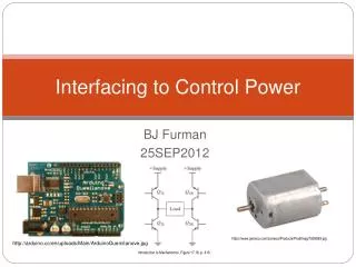
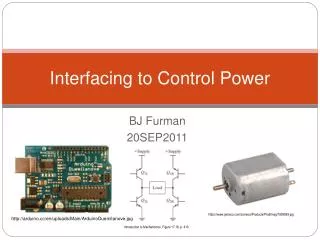
Interfacing to Control Power. BJ Furman 20SEP2011. https://www.jameco.com/Jameco/Products/ProdImag/1939589.jpg. http://arduino.cc/en/uploads/Main/ArduinoDuemilanove.jpg. Introduction to Mechatronics, Figure 17.16, p. 410. Outline. Learning objectives Context for this module Diodes

Interfacing to Control Power
E N D
Presentation Transcript
Interfacing to Control Power BJ Furman 20SEP2011 https://www.jameco.com/Jameco/Products/ProdImag/1939589.jpg http://arduino.cc/en/uploads/Main/ArduinoDuemilanove.jpg Introduction to Mechatronics, Figure 17.16, p. 410.
Outline BJ Furman SJSU Mechanical and Aerospace Engineering ME 106 Learning objectives Context for this module Diodes Bipolar junction transistors (BJT) MOSFETs Using transistors to control power
Learning objectives BJ Furman SJSU Mechanical and Aerospace Engineering ME 106 Explain the theory, construction, and behavior of a diode Explain the theory, construction, and behavior of a bipolar junction transistor (BJT) Explain the theory, construction, and behavior of a MOSFET Design an interface between a microcontroller and device that needs significant power
PowerSource SignalConditioning PowerInterface UserInterface Actuator Sensor System toControl ME 110 ME 136 ME 154 ME 157 ME 182 ME 189 ME 195 Context for this module Mechatronics Concept Map ME 106 ME 120 ‘Muscle’ Controller(Hardware & Software) ME 30 ME 106 ME 190 ME 187 ME 106 INTEGRATION ME 106 ME 120 ME 106 ME 154 ME 157 ME 195 ME 120 ME 284 BJ Furman 22JAN2011 BJ Furman SJSU Mechanical and Aerospace Engineering ME 106
Diode Types and Circuit Symbols • Diode Types • Signal Diodes • Rectifier Diodes • Light Emitting Diodes • Zener Diodes Symbol: Anode(P) Cathode(N) Actual Device: Anode(P) Cathode(N) BJ Furman SJSU Mechanical and Aerospace Engineering ME 106
P-N Junction – Forward Bias A Diode is formed by A junction between positively and negatively doped semiconductor material • P Type • Doped with Boron or Gallium(1 Less e-) • N Type • Doped with Arsenic or Phosphorous(1 Extra e-) Anode(P) Cathode(N) P N Holes e- Net current + - BJ Furman SJSU Mechanical and Aerospace Engineering ME 106
P-N Junction – Reverse Bias • P Type • Doped with Boron or Gallium(1 Less e-) • N Type • Doped with Arsenic or Phosphorous(1 Extra e-) Anode(P) Cathode(N) P N Holes e- No net current -+ BJ Furman SJSU Mechanical and Aerospace Engineering ME 106
I-V Characteristic for a Diode (non-linear) Anode(P) Cathode(N) = 1/R I IV Characteristic for a Resistor Reverse Bias Cathode voltage higher than anode voltage V Breakdown Voltage50-1000V 0.6 to 0.7 V for silicon diode, For LED ~ 1.5 V (IR) – 3.8 V (Blue) Forward Bias Anode voltage higher than cathode voltage Why do you need a resistor in series with a diode? BJ Furman SJSU Mechanical and Aerospace Engineering ME 106
I-V Characteristic for a Zener Diode Anode(P) Cathode(N) BJ Furman SJSU Mechanical and Aerospace Engineering ME 106 Introduction to Mechatronics, Figure 10.8, p. 203.
Diode Example 1 • Find VD, IR, VR + VD - - 10V + + VR- IR VD = -10V, VR = 0, IR = 0 BJ Furman SJSU Mechanical and Aerospace Engineering ME 106
Diode Example 2 • Find VD, IR, VR , R = 1Ω VD= 0.7V VR = 10 – 0.7 = 9.3V IR = 9.3 / 1 =9.3A + VD - + 10V - + VR- IR BJ Furman SJSU Mechanical and Aerospace Engineering ME 106
Diode Applications + VD - • Full wave - 10V + + VR- ~ IR BJ Furman SJSU Mechanical and Aerospace Engineering ME 106 • AC Rectification • Half wave
Bipolar Junction Transistor (BJT) Introduction to Mechatronics, Figure 10.15, p. 206. • So,B-C and B-E junctions look like…? • Remember this! BJ Furman SJSU Mechanical and Aerospace Engineering ME 106 Construction and schematic
BJTOperation (conceptual) Introduction to Mechatronics, Figure 10.16 p. 206. Key concepts • Must turn on B-E diode to get C-E current • Ic = hfeIB (up to saturation) Introduction to Mechatronics, Figure 10.17 p. 207. BJ Furman SJSU Mechanical and Aerospace Engineering ME 106 • Like a current-controlled valve where base-emitter current controls collector-emitter current • Hydraulic analogy for NPN • How much ‘pressure’ (i.e., voltage, VBE) is needed to cause iBE?
BJTlow-side drive Consider hfe= 100 (current gain) V+= 12 V Vce(sat)= 0.3 V RB= 10 kohms Rload=500 ohms Plot Vce, Ic, Pt, and Pload vs. Vin Introduction to Mechatronics, Figure 10.18 p. 207. BJ Furman SJSU Mechanical and Aerospace Engineering ME 106 • For mechatronics, transistors are mostly used as electronically controlled switches • Either fully off (cut off) or fully on (saturated) • Want to avoid the in-between condition (linear region). Why…? • Minimize power dissipation in the transistor
BJTlow-side drive example Procedure • Work backward starting with the load • What Ic is needed for saturation? • Find a transistor that will handle Ic and V+ (data sheet) • Determine hfe and Vce(sat) at Ic(sat) from the data sheet • Determine iB(minimum) to saturate the transistor: • Select RB to give iB with some extra margin (2x – 10x): Introduction to Mechatronics, Figure 10.18 p. 207. BJ Furman SJSU Mechanical and Aerospace Engineering ME 106 • Find RB to turn on the lamp (Rload) • R= 100 ohms • Vce(sat)= 0.3 V • V+= 10 V • Vin = 3.3 V
BJThigh-side drive Introduction to Mechatronics, Figure 10.23 p. 210. BJ Furman SJSU Mechanical and Aerospace Engineering ME 106 • Uses a PNP transistor • Turn on by making Vin at least 0.6 V lower than V+ • Turn off by making Vin at least 0.6 V higher than V+
The Darlington pair Introduction to Mechatronics, Figure 10.24 p. 211. ST TIP120 data sheet Motorola ULN2803 data sheet BJ Furman SJSU Mechanical and Aerospace Engineering ME 106 • Provides higher current gain • For NPN VBE will be about 1.2 V • Current gains in saturation are about 200 to 500:1 • Popular versions • TIP100 series • TIP120 • ULN2803 Octal driver
The MOSFET Introduction to Mechatronics, Figure 10.27 p. 213. Introduction to Mechatronics, Figure 10.28 p. 213. BJ Furman SJSU Mechanical and Aerospace Engineering ME 106 • Metal Oxide Semiconductor Field Effect Transistor • Distinctions from BJT • Voltagecontrolled, rather than current controlled as for the BJT • Conduction path (D-S) behaves like a small resistance rather than a fixed voltage drop when fully on • Enhancement and depletion types • Gate-source voltage controls drain-source current • N-channel (enhancement) fully turns on when VGS > VOn • VOn = 4.5 V for logic-level types, 10 V for non-logic level types • P-channel (enhancement) turns on when VSG > VOn • RDS drops to a relatively low value when device is fully on • mOhms for power MOSFETs
The MOSFET (hydraulic analogy) Introduction to Mechatronics, Figure 10.29 p. 213. BJ Furman SJSU Mechanical and Aerospace Engineering ME 106 • Gate to source ‘pressure’ (voltage) controls drain-source flow restriction (RDS) • Small gate capacitance • Small transient current to build up VGS, but none needed in steady state
MOSFET high and low-side drive examples Low-side drive Introduction to Mechatronics, Figure 10.32 p. 215. High-side drive Introduction to Mechatronics, Figure 10.33 p. 216. BJ Furman SJSU Mechanical and Aerospace Engineering ME 106 • Low-side drive • Use an N-channel MOSFET • For ‘logic level’ MOSFET, VGS should be about 5 V to achieve low RDSon • For regular power MOSFET, VGS should be about 10 V to achieve low RDSon • High-side drive • Use a P-channel MOSFET • For ‘logic level’ MOSFET, VGS should be about -5 V to achieve low RDSon • For regular power MOSFET, VGS should be about -10 V to achieve low RDSon
BJT vs. MOSFET – which to use? BJ Furman SJSU Mechanical and Aerospace Engineering ME 106 • Depends on how much control voltage and current is available • Some overlap where either type could be used • Decide based on cost, complexity, and efficiency • BJT advantages • When control voltage is relatively small (i.e., less than 3 V) • Higher voltage switching capability • MOSFET advantages • When lowest voltage drop or lowest power dissipation across the switch is required • When sufficient voltage is available, but not sufficient control current • Gate drivers are available (ex. LTC1157) • Less complex (no extra resistor), but may be more expensive
Switching loads with having appreciable inductance BIG Problem! Introduction to Mechatronics, Figure 23.1 p. 553. Introduction to Mechatronics, Figure 23.4 p. 553. BJ Furman SJSU Mechanical and Aerospace Engineering ME 106 • You must protect the transistor switch from transient voltages when driving inductive loads • Motors, solenoids, etc. haverelatively large inductance • Inductance is analogous to…? • Inertia • Problem arises when turning the switch off • Collapsing magnetic field will create a transient voltage spike • Ex. L=200 mH, 0.65 A, 1ms switching time • Need a way to dissipate the energy • Use a diode (at the very least) • Diode plus Zener diode or TVS diode better
Choosing the transient suppression components Introduction to Mechatronics, Figure 23.4 p. 553. Introduction to Mechatronics, Figure 23.7 p. 558. BJ Furman SJSU Mechanical and Aerospace Engineering ME 106 • Simple diode • Fast recovery time, trr • A few hundred nanoseconds or less • Ex. 1N4933 • Select diode so that its peak intermittent current is greater than the maximum current you need to switch off • Simple diode plus Zener diode • Choose the Zener so that its reverse-breakdown voltage does not exceed the VCE or VDS maximum of the transistor and that it can handle the maximum current that will be switched off • TVS diodes • http://www.littelfuse.com/data/en/Product_Catalogs/Littelfuse_TVS_Diode_Catalog.pdf
PWM on the mbed BJ Furman SJSU Mechanical and Aerospace Engineering ME 106 • Six PWM channels • p21-p26 • All channels share the same period • Default is 0.02 s • Default pulsewidth is 0 s • What is the default duty cycle? • LED1-LED4 share p26-p23 respectively, so you can brighten or dim them
PwmOut Class BJ Furman SJSU Mechanical and Aerospace Engineering ME 106
mbed overview http://mbed.org/media/uploads/simon/mbedmicrocontrollerpinout4.png BJ Furman SJSU Mechanical and Aerospace Engineering ME 106
mbedpinouts http://mbed.org/media/uploads/Lerche/lpc1768_pin_functions.gif BJ Furman SJSU Mechanical and Aerospace Engineering ME 106
http://www.synvox.ch/lpc1768/lpc1768_mbed_pinout.pdf BJ Furman SJSU Mechanical and Aerospace Engineering ME 106
Starboard Orange http://mbed.org/cookbook/StarBoard-Orange BJ Furman SJSU Mechanical and Aerospace Engineering ME 106
For More Information BJ Furman SJSU Mechanical and Aerospace Engineering ME 106 • Mabuchi Motor Technical Reference http://www.mabuchi-motor.co.jp/en_US/technic/index.html • DC Motor Tutorials from MicroMo http://www.micromo.com/dc-motor-tutorials.aspx • Maxon Motor Academy http://www.maxonmotor.com/maxon-academy.html • Maxon Motor e-Catalog http://www.maxonmotor.ch/e-paper/