Download

1 / 14
140 likes | 159 Views
JRA3 DAQ Overview. Matt Warren, on behalf of EUDET JRA3 DAQ Groups. Please see the following talks from the JRA3 Parallel Session for more detail: DAQ and DIF - Bart Hommels DIF controls - Maurice Goodrick DIF-LDA interface and LDA hardware - Marc Kelly. Reminder: The PLAN.

E N D
JRA3 DAQ Overview Matt Warren, on behalf of EUDET JRA3 DAQ Groups. Please see the following talks from the JRA3 Parallel Session for more detail: DAQ and DIF - Bart Hommels DIF controls - Maurice Goodrick DIF-LDA interface and LDA hardware - Marc Kelly
Reminder: The PLAN • Use commercial components where possible: • Readout links use standard connectors and protocols • PCs with PCI (-Express) cards • Modular/Generic Structure • Generic readout system as much as possible • Detector specific interfaces only at ends of chain • Other ‘bespoke’ functionality in firmware • Clock and Control attempts commercial hardware too • Extract ‘fast’ signals from commercial signalling • DAQ software generic for all detectors • Try use something off-the-shelf … Matt Warren - JRA3 DAQ Overview
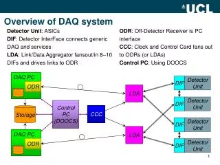
Host PC Host PC ODR ODR PCIe PCIe DIF DIF DIF DIF Detector Unit Detector Unit Detector Unit Detector Unit DAQ architecture Detector Unit: ASICs DIF: Detector InterFace connects Generic DAQ and services LDA: Link/Data Aggregator – fanout/in DIFs and drives link to ODR ODR: Off Detector Receiver – PC interface for system. C&C: Clock & Control: Fanout to ODRs (or LDAs) LDA C&C Storage LDA Matt Warren - JRA3 DAQ Overview
Host PC ODR PCIe ODR (Off Detector Receiver) • ODR receives data from LDA and transfers controls and config to LDA for distribution. • Commercial FPGA dev-board • PLDA XPressFX100 – Virtex 4, 2xSFP, 8xPCIe • Our own firmware and driver software • Stage 1 firmware & software working: • Data received via GigE (optical), buffered and transferred to disk. • Performance studies & optimisation on-going • Stage 2 starting: • Config + controls source (e.g talk to LDA) • More channels (4-5) • Use external DDR2 RAM • Additional hardware recently purchased to cover multi-link tests and initial user needs Storage Matt Warren - JRA3 DAQ Overview
LDA (Link/Data Aggregator) Fans-out C+C+C to detector Fans-in data to ODR • Commercial FPGA dev-board (Enterpoint Broaddown2) • Spartan3-2000 • 2 add-on boards specifically for our needs: - SPF+SerDes for ODR link - 10 HDMI connectors, clock/signals fanout • USB interface for stand-alone/top-of-chain testing LDA LDA Matt Warren - JRA3 DAQ Overview
DIF Detector Unit DIF (Detector InterFace) • FPGA + detector hardware connected to Detector Unit. • Two halves – Generic DAQ and Specific Detector • 3 detectors: ECAL, AHCAL, DHCAL • 1 DAQ Interface! Focusing on the DAQ side: • From LDA, receive, decode/regenerate and distribute clocks, fast commands, config data and slow controls. • From ASICs, receive, buffer, package and forward data to LDA • ALSO: USB interface - On DAQ AND Detector sides! • Hardware designers already have one • DAQ plans to integrate for stand-alone tests DAQ USB Matt Warren - JRA3 DAQ Overview
DIF DIF DIF DIF Detector Unit Detector Unit Detector Unit Detector Unit LDA-DIF link • Serial link running at multiple of machine clock • ~50Mbps (raw) bandwidth minimum • robust encoding (8B/10B or alike) • HDMI cables/connectors interface. • Commercially available cables • Even halogen free (e.g. Van Den Hull) • Signals: Clock (diff) Control/Fast (diff) Very Fast (diff) Data (diff) single ended aux x2 (or UTP) • LDAs serve even/odd DIFs for redundancy LDA LDA Matt Warren - JRA3 DAQ Overview
Host PC Host PC ODR ODR PCIe PCIe Clock & Control • C&C unit provides machine clock and fast signals to ODR, LDA. • Stand-alone, dumb, hardware • But capable of external control • Provision for async scintillator type signals (VFast) • LDA provides fanout to DIFs • Requirements for non-JRA3 users?? • Clock jitter requirement? • VFast trigger latency? LDA C&C LDA • Fast Controls: encoded commands on the LDA-DIF link • Slow Controls/Configuration: transfers on LDA-DIF link • VFast signals: distributed ‘directly’ (if necessary) Matt Warren - JRA3 DAQ Overview
Clock & Control Detail AUTO / X-TAL SW-0 A) CLOCK LVDS on SMA EXT.CLKIN 8x LVDS on HDMI 1 OR LVTTL on Lemo (8x LVDS on SMA ? ) NIM on Lemo MPX +PLL 2x LVTTL on Lemo 2x NIM on Lemo ~ 50 MHz X-TAL B) FAST TRIG SW-1 2->1 LVDS on SMA 8x LVDS on HDMI C) CONTROLS ( 1xLVDS TRIGGERon RJ-45 ? ) 4x LVDS on SMA 4x NIM on Lemo SW-2 5->1 4x 4 4 8x LVDS on HDMI D) BUSY LVDS on SMA 1 1 SW-3 2->1 8x LVDS on HDMI NIM on Lemo OR 8 o/c TTL on Lemo 4 8 1 1 MP + MW, UCL, 03-10-2007 PCB-1 HEADER / CONNECTOR Matt Warren - JRA3 DAQ Overview
Overall Status/Schedule ODR: Stage 1 complete – Ethernet based read-out link • Stage 2 starting – Control up-link + more channels • Receiver ready now. Bi-directional Q2 2008 LDA: main hardware purchased, DIF/ODR interface hardware add-ons in-progress at manufacturer. • Interfaces specified • Working prototype Q2 2008 DIF: Generic DAQ Interfaces mostly defined, plenty of detector specific interfaces C&C: Hardware design in progress now – Comments?? - Hardware for Q1 2008 Software: -See next talk! Schedule: - Development prototypes mid-2008 - FULL DAQ mid-2009 Matt Warren - JRA3 DAQ Overview
Extra: C+C Draft Proposal: Matt Warren - JRA3 DAQ Overview
CALICE C&C PROPOSAL DRAFT -4-FOR COMMENTS & CORRECTIONS A) CLOCK : a) 3x EXTERNAL INPUTS : 1) 1x Diff. LVDS ( 2x SMA ) 2) 1x LVTTL/CMOS (?) ( 1x Lemo 00 ) 3) 1x NIM ( 1x Lemo 00 ) b) INTERNAL X-TAL OSCILLATOR ( 100MHz clk ) - Inputs a1+a2+a3 converted to single-ended LVTTL/CMOS (?) level All three plain OR-ed together to produce single EXT-CLK-IN b) output divided-by-two to produce INT-CLK at 50MHz, LVTTL/CMOS (?) - EXT-CLK-IN and INT-CLK input into Mux-PLL ( ICS581 ? ) to produce single clock CLK-OUT, automatically switching from EXT-CLK-IN to INT-CLK if external clock missing for > 3 periods - Hardware switch SW-0 to force Mux. to switch to 50MHz INT-CLK input - Mux-PLL output : 45min/55max Duty Cycle +/- 150ps max absolute period jitter CLK-OUT OUTPUTS : 1) 8/10/12x Diff. LVDS outputs ( on HDMI each ) 2) [ 8/10/12x Diff. LVDS outputs ( 2x SMA each ) ?? ] 3) 2x LVTTL/CMOS (?) ( 1x Lemo 00 each ) 4) 2x NIM ( 1x LEMO 00 each ) 5) 1x Diff. LVDS on PCB-1 Header ( see below ) Matt Warren - JRA3 DAQ Overview
B) FAST TRIGGER : 1x FAST TRIGGER INPUT : 1x Diff. LVDS ( 2x SMA ) - Input B1) passed straight onto a dual rotary-selector switch or header/jumper selector SW-1 - Input B1) passed also onto the PCB-1 Header as 1x Diff. LVDS output ( see below ) 8/10/12x FAST TRIGGER OUTPUTS : 1) 8/10/12x Diff. LVDS outputs ( on HDMI each ) produced from the output of the selector SW-1from either the Input A or from Input AP on the PCB-1 Header ( see below ) C) CONTROLS : c) 3x EXT. TRIGGER INPUTS : 1) 1x Diff. LVDS ( 2x SMA ) 2) 1x NIM ( 1x Lemo 00 ) 3) [ 1x Diff. LVDS ( 1x PJ-45 ) ?? ] d) 2x EXT. START INPUTS : 1) 1x Diff. LVDS ( 2x SMA ) 2) 1x NIM ( 1x Lemo 00 ) e) 2x EXT. AUX-1 INPUTS : 1) 1x Diff. LVDS ( 2x SMA ) 2) 1x NIM ( 1x Lemo 00 ) f) 2x EXT. AUX-2 INPUTS : 1) 1x Diff. LVDS ( 2x SMA ) 2) 1x NIM ( 1x Lemo 00 ) - Each set of Inputs c1+c2+c3, d1+d2, e1+e2, f1+f2 are OR-ed together, producing single-ended signals c12, d12, f12. f12 - Each line c12, d12, e12, f12 ends with rotary-selector switch or header/jumper selector SW-2 - Each line c12, d12, e12, f12 passed also onto the PCB-1 Header as single-ended outputs ( see below ) 8/10/12x CONTROL OUTPUTS : 1) 8/10/12x Diff. LVDS outputs ( on HDMI each ) - produced from the output of the selector SW-2 from either the four inputs c12, d12, e12, f12 or from single Input CONTROL-P on the PCB-1 Header ( see below ) Matt Warren - JRA3 DAQ Overview
D) BUSY FEEDBACK : 8/10/12x BUSY FEEDBACK INPUTS : 1) 8/10/12x Diff. LVDS ( on HDMI each ) - All 8/10/12x inputs sent to the PCB-1 Header ( see below ), as well as being all OR-ed with the single output BUSY sent to a switch-selector or header/jumper SW-3 ( see below ) 3x BUSY OUTPUTS : 1) 1x Diff. LVDS ( 2x SMA ) 2) 1x NIM ( 1x Lemo 00 ) 3) 1x o/collector TTL ( 1x Lemo 00 ) - BUSY OUTPUTs produced from the output of the selector SW-3 from either the single BUSY input or from single input BUSY-P on the PCB-1 Header ( see below ) PCB-1 HEADER : standard 0.1" dual PCB Header to provide connections to a control/ODR PCB for possible processing of signals on FPGA PCB-1 Header carries the following lines : - one pair Diff. LVDS line CLK-OUT output - one pair Diff. LVDS line A Fast Trigger output - one pair Diff. LVDS line AP Fast Trigger input - four c12, d12, e12, f12 single-ended CONTROL outputs - one single-ended CONTROL-P input - 8/10/12 single-ended BUSY-N outputs - one single-ended BUSY-P input POWER : It is proposed to have an external P/S, connected to the C&C PCB by a DC power socket Matt Warren - JRA3 DAQ Overview