HCAL TriDAS Readout Crate Components Overview
Explore the components and functionalities of the HCAL TriDAS Readout Crate, including the Trigger Primitive Generator and Data Acquisition System. Learn about the FPGA logic implementation, data transmission paths, and the status of the demonstrator. Stay updated on the firmware development and progress towards testbeam readiness.

HCAL TriDAS Readout Crate Components Overview
E N D
Presentation Transcript
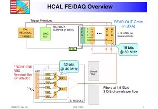
Trigger Primitives READ-OUT Crate (in UXA) DAQ DATA SLINK64 [1 Gbit/s] CAL REGIONAL TRIGGER CPU D C C H T R H T R H T R DAQ RUI 18 HTRs per Readout Crate 16 bits @ 80 MHz TTC 32 bits @ 40 MHz CCA CCA CCA FRONT-END RBX Readout Box (On detector) HPD Shield Wall QIE GOL QIE QIE Fibers at 1.6 Gb/s 3 QIE-channels per fiber QIE GOL QIE QIE FE MODULE HCAL FE/DAQ Overview HCAL TriDAS
Readout Crate Components • “BIT3” board • Commercial VME/PCI Interface to CPU • Slow monitoring • HTR (HCAL Trigger and Readout) board • FE-Fiber input • TPs output (SLBs) to CRT • DAQ/TP Data output to DCC • Spy output • TCC/Clock FanOut board • FanOut of TTC stream • FanOut of RX_CK & RX_BC0 for SLBs • DCC (Data Concentrator Card) board • Input from HTRs • Output to DAQ • Spy output Front End Electronics TTC fiber Gbit Ethernet @ 1.6 Gb/s F a n O u t B I T 3 H TR H T R H T R H T R D C C (s) ... D C C 20 m Copper Links 1 Gb/s DAQ Calorimeter Regional Trigger HCAL TriDAS
HCALTRIGGERandREADOUTCard • No functional changes since Dec-2001 • I/O on front panel: • Inputs: Raw data: • 16 digital serial fibers from QIE, 3 HCAL channels per fiber = 48 HCAL channels • Inputs: Timing (clock, orbit marker, etc.) • PECL • Outputs: DAQ data output to DCC • Two connector running LVDS • TPG (Trigger Primitive Generator, HCAL Tower info to L1) via P2/P3 • Via shielded twisted pair/Vitesse • Use aux card to hold Tx daughterboards • FPGA logic implements: • Level 1 Path: • Trigger primitive preparation • Transmission to Level 1 • Level 2/DAQ Path: • Buffering for Level 1 Decision • No filtering or crossing determination necessary • Transmission to DCC for Level 2/DAQ readout HCAL TriDAS
Demonstrator Status • HTR Demonstrator DONE • Consists of 2 boards: • 6U HTR receiver board • Front-end emulator transmitter board • Functions implemented: • Data, LHC structure, CLOCK • 800 Mbps HP G-Links works like a champ • Dual LCs • FEE sends clock to HTR, bypasses TTC • HCAL FNAL source calibration studies in hand 6U HTR Receiver 6U FEE Transmitter HCAL TriDAS
Baseline 48 channel HTR • All programmable logic implemented on 2 identical 24-channel subsets: • 8 TI TLK2501 transceivers (3 HCAL channels/fiber) • 4 Strator dual LC optical receivers • Xilinx XCV1000E • TPG output to CRT via SLB • L1A Output to DCC via SLB transition module • FPGA TTL LVDS backplane LVDS TTL • NOTE: DCC bandwidth limitation by PCI • Need 2 DCC/crate • New Xilinx Vertex2 PRO being considered now • Fewer I/O pins required • Discrete serdes requires ~20 pins each, reduced to 1 differential @ 1.6 GHz • Internal clock distribution should work. • Built in Motorola 300MHz PowerPC 405 • We will surely find a use for this! • 1 18-bit hardware multiplier per block ram • Working with the vendors to get engineering sample • Plan to have a board built over the summer for checkout • Tremendous effort by Tullio Grassi VME HCAL TriDAS
HTR Block Diagram • In progress… HCAL TriDAS
Current Status HTR • 1.6 GHz link is the hardest part • Already implemented on in-house “LinkOnly” board • HTR Prototype is on the bench now • Half functionality for 02 testbeam • 1 FPGA • Firmware in progress • 8 serdes • Tested ok. Some VME power supply issues. • DCC output • Already tested • External clock input • VME • Firmware developed at BU, good progress • This board will be cloned for the testbeam effort Dual LC Fiber Detector 8 TI TLK1501 deSerializers Xilinx XCV1000E FPGA HCAL TriDAS
Changes from HTR Prototype to Final FPGA+8 deserializers • TPG transmission changed • From SLB mezzanine cards to Backplane aux card • Solves mechanical problems concerning the large cables to Wesley • 1.6 GHz link • Wider traces, improved ground planes, power filtering, etc. • Deserializer RefClock fanout • TTC daughterboard to TTC ASIC • Fixed TI deserializer footprint problem • Clocking fixes • Next iteration estimate • Submit in 2 weeks • Stuffed and returned • by April 1 VME FPGA Out to DCC TTC and Clock distribution OLD DESIGN Dual LC Fiber Connector HCAL TriDAS
HTR Firmware - VME • All firmware implemented using Verilog implementation • Non Trivial firmware effort underway • 1 engineer, 1 EE graduate student, 1 professor • VME path to HTR implemented via Altera FPGA • BU is developing • Status is good – confidence that this will be ready for testbeam • VME is not too difficult if you don’t have to do DMA, interrupts, etc. • Based on a “LocalBus” model • LocalBus devices are the 2 Xilinx FPGAs, flash eeprom for config over VME, internal VME FPGA device, and the 6 SLB daughterboards MAIN FPGA 1 (Xilinx) Flash Eeprom 1 Altera 10k30 MAIN FPGA 2 (Xilinx) Flash Eeprom 2 VME FPGA (same 10k30) TTC SLB 1 SLB 2 SLB 3 VME SLB 4 SLB 5 SLB 6 LocalBus HCAL TriDAS
HTR Firmware – HCAL functionality • Firmware for this consists of 2 paths: • Level 1 path • Raw QIE to 16-bit integer via LUT • Prepare and transmit trigger primitives • Associate energy with crossing • Extract muon “feature” bit • Apply compression • Level 2 path • Maintain pipeline with L1Q latency (3.2ms) • Handle L1Q result • Form energy “sums” to determine beam crossing • Send L1A data to DCC • Effort is well underway • 1 FTE engineer (Tullio Grassi) plus 1 EE graduate student plus 1 professor • Much already written, ~1000 lines Verilog • Much simulation to do • Focusing now on Level 2 path functions necessary for testbeam Schematic for each of 2 Xilinx FPGA HCAL TriDAS
Clocking • Many clocks in HTR board. • Best to describe in terms of “Tight” and “Relaxed” jitter requirement: • Tight jitter spec: 2 clocks needed • REFCLK for Serdes fiber receivers (TI TLK2501) lock to incoming 1.6 Gbps data • 80MHz • Preliminary REFCLK jitter requirements were surprising… • Measured 30-40ps pkpk jitter needed at input to Serdes on Maryland “eval” board • Measurements on current 9U board underway, maybe it’s not so bad. • Provide transmitter clock for SLB output • 40MHz • Jitter spec is 100ps at Vitesse transmitter • Loose jitter spec: 1 clock needed • TTC-derived system clock for HTR logic • Used only by the FPGA • Implementation described on next slide…. HCAL TriDAS
Quad Twisted Pair Cat 5 LVDS 40MHz RJ45 LVDS 120MHz Clock Implementation - HTR • Tight Jitter clock: • Use same clock for both 80MHz Serdes REFCLK and 40MHz SLB Tx clock • DFF used to divide 80MHz into 40MHz • Clock will be implemented in 2 ways: • Incoming from Clock Fanout Board • PECL fanout, convert to TTL at input to Serdes • Onboard crystal for debugging • Loose Jitter clock • Use TTC clock for 40MHz system clock • Clock will be implemented in 3 ways on HTR: • TTC clock from fanout board • External lemo connector • Backup input from fanout board • 2 RJ45 connectors with Cat 5 quad twisted pair connectors • 1st one has incoming low jitter 80MHz clock from fanout • 3.3V PECL on 1 pair, other 3 pair grounded • 2nd one has: • 120MHz LVDS TTC from fanout board on 1 pair • 40MHz LVDS L1A, Backup clock, and BC0 on other 3 pair L1A CLK BC0 TTC A/B Quad Twisted Pair Cat 5 RJ45 GROUND 80MHz CLK GROUND GROUND HCAL TriDAS
HTR/Clock Implementation • In progress… Lemo test inputs….RST, L1A, CLK RJ45 connector with TTC, L1A, BC0, Clock_backup Fanout Buffer RJ45 connector with low jitter PECL 80MHz clock HCAL TriDAS
Optic Fiber Input VME64x connector Cat 5/RJ45 LVDS fanout TTCrx daughter card HCAL Fanout Prototype Board • Fanout card handles requirement for • TTC fanout • L1A/BC0 fanout for SLB synch • Clock cleanup for low jitter REFCLK • TTC Fanout • Each HCAL VME crate will have 1 TTCrx for all HTR cards • TTC signal converted to 120MHz LVDS, fanout to each HTR and over Cat5 w/RJ45 • L1A, BC0, CLK • Fanout using 40MHz LVDS • CLK is just for test/debugging • Clock Cleanup • Cleanup the incoming 80MHz TTC clock using VCXO PLL • Fanout to HTR • Status • Prototype board checked out ok • 3 production boards due next week HCAL TriDAS
120MHz LVDS TTC 40MHz LVDS BC0/L1A/CLK REDUNDANCY 6U Clock Board Fanout Board HTR Board SLB Transition Board LEMO deserializers 40MHz TTCrx LVDS TTCrx CLK “CLK” 1 to 8 Fanout BC0 L1A 80 MHz 80MHz 1 to 8 Fanout 80 MHz LVPECL Crystal 80 MHz PECL PECL 80MHz Clock Fanout 40 MHz Clean 80MHz Clock REDUNDANCY RJ45 Splitter REDUNDANCY Testbeam Clocking Scheme • UIC Clock Fanout Board • Fanout “clean” 80MHz PECL clock • Fanout TTC to all HTR via LVDS • 80MHz clean clock redundancy • HTR • 80MHz clean clock for Serdes REFCLK redundancy • 40MHz TTC sysclock, L1A and BC0 • Single clock source: 6U Princeton Clock Board • Source of clean 40MHz clock for TTCvx • Redundant 80MHz clock • TTCvx • Fiber output TTC HCAL TriDAS
TPG Output to Level 1 • HTR cards will send data to Dasilva’s SLB boards • Quad Vitesse transmitter, 40MHz clean clock input (100ps jitter) • Mechanical considerations dictated design of 6-SLB transition board (SLB_HEX) • Baseline scheme: 6-SLB transition motherboard (SLB_HEX) • HTR will send 280 MHz LVDS across backplane • SLB_HEX will fanout 40MHz clean clock and have LVDS-to-TTL drivers • 6 SLB=48 TPG matches HTR “magic number” 3 HCAL channels/fiber input • Risks: lots of LVDS, but Dasilva is confident! • Alternate schemes under consideration • Move SLB’s to HTR • Mechanically challenging – heavy TPG cables • This is our main backup • Build 9U “super” SLB motherboard • Not sure if this helps…. • Build 6U crate of super SLB motherboards • Same thing…. HCAL TriDAS
Adding HO to RPC Trigger • Considerations: • Requirements • Trigger would only need 1 bit per HCAL tower • RPC trigger accepts 1.6 Gbps GOL output • Technical – how hard will it be to do this? • 48 channel HTR means 48 bits/HTR to RPC trigger • Each SLB twisted pair sends 24 bits @ 120MHz • Entire output could go via a single SLB • Can the SLB output be modified to drive fiber? • Can the RPC trigger receiver be modified to accept 1.2 GHz? • Under study….will try to come up with a decision this month • Mapping • HCAL mapping is very constrained (ask Jim Rohlf!) • Can we map our towers/fibers to the RPC? • Maybe easy for f • Maybe hard for h • Rohlf to study this…. HCAL TriDAS
Project Development • Demonstrator Stage • Demonstrated scaled down system • FE (800 MHz) (6U, Altera) “DCC” CPU • Nothing in the way of pipeline, TPG, derandomizer, preDCC logic board, etc. • Testbeam 2002 Stage • Demonstrate full 9U system • FE (1.6 GHz, real RBX) HTR (9U, Xilinx, TTC…) DCC (full logic board) CPU • Main goals are to learn about HCAL data, gain experience with clocking, produce fully integrated system • Pipelining/derandomizer but no TPG, and certainly not final CMS/LHC-ready firmware • Summer 2003 • Integration with L1Trigger, DAQ, VME rack support requirements • Vertical Slice 2004 • Full integration HCAL TriDAS
Done Test Beam Jul-Sep FNAL source calib. Current Project Timeline 2001 2002 2003 2004 2005 Demonstrator HTR Firmware Development…. Pre-production Prototype 1.6 Gbps Link 9U Prototype Testbeam Firmware TPG/LVDS Checkout 9U Prototype HTR Production Alcove/Slice Integration Install • Uncertainties • Vertex-2 or Vertex-2 PRO • Global clocking scheme • Clock jitter • SLB motherboard HCAL TriDAS
Integration/Installation/Commissioning • First HTR/DCC integration completed • Jan 2001 FNAL source calibration test • HTR (6U Altera demonstrator) LVDS DCC SLINK CPU • Physical link from HTR to DCC established • Next integration will take place during the Summer 2002 testbeam • 9U HTR, Xilinx, more mature firmware… • 35MHz test of physical optical link from HCAL front-end to HTR • More of a firmware integration between HTR and DCC • Integration with Level 1 to commence Q4 2002 after… • Checkout of HTR Channel-Link over backplane to SLB_HEX/SLB • Receipt of Wisconsin Vitesse VME receiver boards, fall 2002 • We should be confident of ability of HTR to send synchronized data to L1 before going to pre-production prototype HCAL TriDAS
Integration/Installation/Commissioning(cont) • Summer 2003 testbeam • Mostly firmware integration • 2003 Level 1 trigger installation • HCAL will join as schedule allows • Probably not until after the testbeam • 2003/2004 HCAL burning • Continue with firmware development/integration as needed • 2004/2005 Vertical Slice and magnet test • We will be ready • All HCAL TriDas production cards involved • October 05 beneficial occupancy of USC • Installation of all racks, crates, and cards • We do not anticipate any hardware integration • Should be all firmware / timing / troubleshooting • Need to understand whether we will need large-scale front-end emulation • Current FEE can feed optical data into only a few HTR cards at a time HCAL TriDAS
Installation Manpower Needs • Drawing on D Level 2 experience for the current Tevatron Run 2a… • Each significant card requires on-site expertise: • Probably 1-2 postdoc-level (or above) and 1 engineer • Maybe the same engineer for both DCC and HTR… • HCAL will have an electronics setup at CERN • Total personnel estimate: • Front End 1 • HTR 2 • DCC 2 • Miscellaneous (grad students, transients, etc.) maybe 4? • Very difficult to say with any accuracy HCAL TriDAS