Download

1 / 7
80 likes | 280 Views
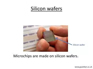
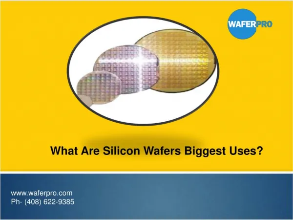
Silicon wafers are made up of a thin slice of silicon that can be altered to make it work in different ways for various types of electronics. Since silicon is considered to be a high-ranking type of semiconductor, it can serve multiple purposes in its wafer form. To get more information please visit www.waferpro.com

E N D
Overview Silicon wafers are made up of a thin slice of silicon that can be altered to make it work in different ways for various types of electronics. Since silicon is considered to be a high-ranking type of semiconductor, it can serve multiple purposes in its wafer form. Wafers are created through the lab-grown crystal growing process, controlling various levels of purity depending upon the final result desired. It is then cut into very thin slices and polished before being used.
Integrated Circuits Silicon is a high-quality semiconductor, and its primary use in wafer form is to serve as a key player in integrated circuits. Integrated circuits are essential to power many of our electronic necessities like computers and cell phones. An integrated circuit can be installed not only around a silicon wafer, but also upon it or inside of it. Silicon wafers used for integrated circuiting are usually designed in the southern part of the San Francisco Bay area, more commonly known as Silicon Valley. Here you will find the home bases of many big names in technology including Google, Apple and Oracle.
Solar Cells Silicon wafers are used to produce solar cells, also known as photoelectric cells. This final product is able to convert light energy into electricity. Types of artificial light are also able to be used in solar cells, which are then known instead as photovoltaic cells. Silicon acts as a semiconductor by absorbing the photons in sunlight that shine against the solar panel. This in turn creates electricity. However, wafers are quickly being replaced with silicon thin films, which are less bulky and more affordable to produce and use.
Effect of Silicon Wafer Use The use of silicon wafer use has allowed technology to advance by leaps and bounds. It has also created countless jobs for individuals both on the manufacturing and design side. Silicon Valley contains a large percentage of wealthy residents thanks to the discovery and everyday manufacturing of silicon wafers. Unfortunately, the production of silicon wafers, despite its important purpose, has also caused controversy as it has a profound effect on pollution levels.
Wafers Variants While all silicon wafers are useful, it is important to note there are different variations used for various purposes. The P-Type wafer is doped with boron and used for lithography. N-Type wafer have phosphorus and/or arsenic infused in them, and they are then used for advanced CMOS device fabrication. Wafers are measured for flatness and thickness to determine what it can be used for.
Contact us 410 E Santa Clara St # 518, San Jose, CA, USA 95113 sales@waferpro.com (408) 622-9129 www.waferpro.com