Download
1 / 15
190 likes | 502 Views
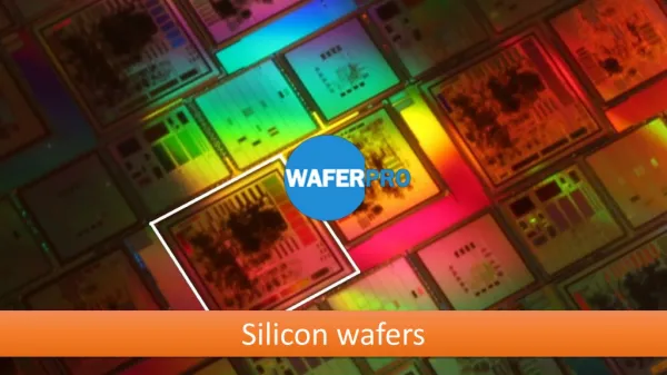
Addison Engineering leading supplier of silicon wafers, wafer processing, semiconductor Equipment, Ceramic Packages, Wafer fabrication, chip carriers and operation Management

E N D
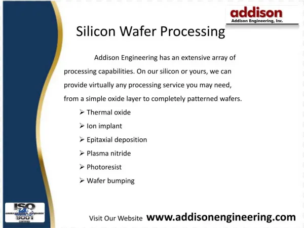
Silicon Wafer Processing • Addison Engineering has an extensive array of processing capabilities. On our silicon or yours, we can provide virtually any processing service you may need, from a simple oxide layer to completely patterned wafers. • Thermal oxide • Ion implant • Epitaxial deposition • Plasma nitride • Photoresist • Wafer bumping Visit Our Website www.addisonengineering.com
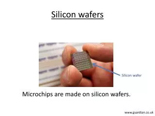
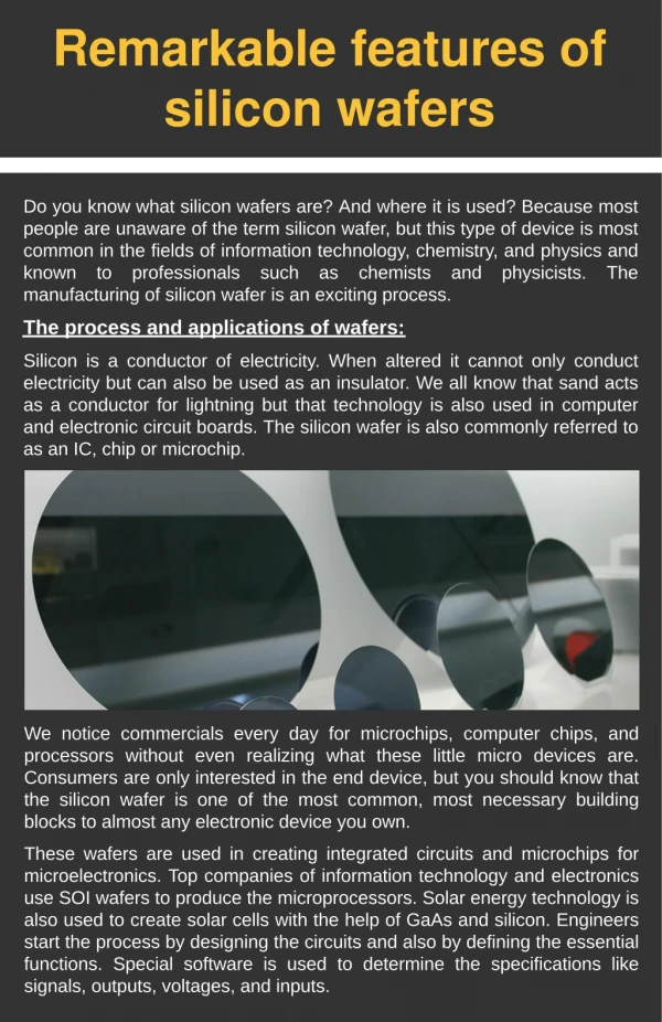
Silicon Wafer Processing About Wafers: In electronics, a wafer (also called a slice or substrate) is a thin slice of semiconductor material, such as a silicon crystal, used in the fabrication of integrated circuits and other microdevices. The wafer serves as the substrate for microelectronic devices built in and over the wafer and undergoes many microfabrication process steps such as doping or ion implantation, etching, deposition of various materials, and photolithographic patterning. Visit Our Website www.addisonengineering.com
Silicon Wafer Processing • Formation: • Wafers are formed of highly pure (99.9999999% purity) nearly defect free single crystal material. • One process for forming crystalline wafers is known as Czochralski growth invented by the Polish chemist Jan Czochralski. • In this process, a cylindrical ingot of high purity monocrystalline semiconductor, such as silicon or germanium, is formed by pulling a seed crystal from a 'melt'. Visit Our Website www.addisonengineering.com
Silicon Wafer Processing • Donor impurity atoms, such as boron or phosphorus in the case of silicon, can be added to the molten intrinsic material in precise amounts in order to dope the crystal, thus changing it into n-type or p-type extrinsic semiconductor. Visit Our Website www.addisonengineering.com
Silicon Wafer Processing • Thermal oxide: • Oxide • TEOS/PETEOS oxide • Gate oxide • Low temperature oxide • PSG glass • Silicon Nitride • LPCVD • Low Stress • Ultra-low Stress • Polysilicon (undoped) Visit Our Website www.addisonengineering.com
Silicon Wafer Processing • Metal deposition • Evaporation • Sputter • Epitaxial deposition • Ion implantation • SOI • oxidation • wafer bonding • Photolithography Visit Our Website www.addisonengineering.com
Silicon Wafer Processing • Clean • RCA clean • Mechanical • Ingot slicing • Lap & etch • Wafer thinning • Wafer downsize (diameter cut-down) • Wafer dicing Visit Our Website www.addisonengineering.com
Silicon Wafer Processing • Wafer reclaim • Laser marking • Wafer bumping • MEMS - Silicon machining Visit Our Website www.addisonengineering.com
Silicon Wafer Processing • Thin Film Processing: • LOW k • Black Diamond® • Coral® • Spin On • and more • OXIDE: CVD and Thermal • Thick Photoresist & Polymide • High Energy Deep Ion Implant • Nitrides (Si- and O-) Visit Our Website www.addisonengineering.com
Silicon Wafer Processing • Low Stress Silicon Nitride • BPSG, PSG, USG • Amorphous Silicon • Diamond Like Carbon • Polysilicon (Doped and Undoped) • METALS: PVD, CVD, Electroplate • Ai, Cu, Au, Cr, Ta, Ti, TiN • TiW, TaN, WN, Ni, Ru • Co, NiSi, TiO2, Pt Visit Our Website www.addisonengineering.com
Silicon Wafer Processing • Czochralski Growth: Visit Our Website www.addisonengineering.com
Silicon Wafer Processing • Grinding and Slicing: Visit Our Website www.addisonengineering.com
Silicon Wafer Processing • Lapping and Etching: Visit Our Website www.addisonengineering.com
Silicon Wafer Processing • Polishing and Cleaning: Visit Our Website www.addisonengineering.com
Silicon Wafer Processing Addison Engineering provides Silicon wafers that are available with a wide range of characteristics (specifications) to select from. Thank You Visit Our Website www.addisonengineering.com