Download
1 / 7
80 likes | 130 Views
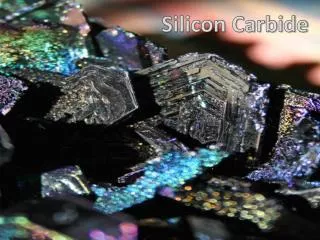
SiC wafer (Silicon Carbide Wafers) is a semiconductor material of ploytype 4H & 6H used in research & manufacturing industries. PWAM develops & produces large size substrates, silicon wafer using high-tech materials in its laboratory. Our main aim is to produce the best silicon wafer for you.<br>http://www.qualitymaterial.net/products.html

E N D
SILICON CARBIDE SUBSTRATES Product Specifications 6H SUBSTRATES 4H SUBSTRATES XIAMEN POWERWAY ADVANCED MATERIAL CO.- NO.99,HULI DEVELOPING ZONE, XIAMEN, 361000,CHINA TEL:+86 (0)592 5601404 -FAX:+86 (0)592 5745822 E-MAIL:SALES@QUALITYMATERIAL.NET WWW.QUALITYMATERIAL.NET
SILICON CARBIDE MATERIAL PROPERTIES Polytype Single Crystal 4H Single Crystal 6H Lattice Parameters a=3.076 Å c=10.053 Å ABCB 3.26 eV 3.21 · 103 kg/m3 4-5× 10⁻⁶/K no = 2.719 ne = 2.777 9.6 490 W/mK 2 – 4 · 108 V/m 2.0 · 105 m/s 800 cm2/V· S 115 cm2/V· S ~9 a=3.073 Å c=15.117 Å ABCACB 3.03 eV 3.21 · 103 kg/m3 4-5×10⁻⁶/K no = 2.707 ne = 2.755 9.66 490 W/mK 2 – 4 · 108 V/m 2.0 · 105 m/s 400 cm2/V· S 90 cm2/V· S ~9 Stacking Sequence Band-gap Density Therm. Expansion Coefficient Refraction Index Dielectric Constant Thermal Conductivity Break-Down Electrical Field Saturation Drift Velocity Electron Mobility hole Mobility Mohs Hardness
6H N-TYPE SIC, 2″ ″ WAFER SPECIFICATION SUBSTRATE PROPERTY S6H-51-N-PWAM-250 S6H-51-N-PWAM-330 S6H-51-N-PWAM-430 Description Polytype Diameter Thickness Carrier Type Dopant Resistivity (RT) Surface Roughness FWHM Micropipe Density Surface Orientation Production Grade 6H SiC Substrate 6H (50.8 ± 0.38) mm (250 ± 25) µm (330 ± 25) µm (430 ± 25) µm n-type Nitrogen 0.02 ~ 0.1 Ω· cm < 0.5 nm (Si-face CMP Epi-ready); <1 nm (C- face Optical polish) <50 arcsec ≤ 30 cm-2 <0001>±0.5° 3.5° toward <11-20>±0.5° On axis Off axis Primary flat orientation Primary flat length Secondary flat orientation Parallel {1-100} ± 5° (16 ± 1.7) mm Si-face:90° cw. from orientation flat ± 5° C-face:90° ccw. from orientation flat ± 5° Secondary flat length Surface Finish Packaging Usable area Edge exclusion (8 ± 1.7) mm Single or double face polished Single wafer box or multi wafer box ≥ 90 % 1 mm
6H SEMI-INSULATING SIC, 2″ WAFER SPECIFICATION SUBSTRATE PROPERTY S6H-51-SI-PWAM-250 S6H-51-SI-PWAM-330 S6H-51-SI-PWAM-430 Description Polytype Diameter Thickness Resistivity (RT) Surface Roughness FWHM Micropipe Density Surface Orientation Production Grade 6H SEMI Substrate 6H (50.8 ± 0.38) mm (250 ± 25) µm (330 ± 25) µm (430 ± 25) µm 90% >1E5 Ω· cm < 0.5 nm (Si-face CMP Epi-ready); <1 nm (C- face Optical polish) <50 arcsec ≤ 50 cm-2 <0001>±0.5° 3.5° toward <11-20>±0.5° Parallel {1-100} ± 5° On axis Off axis Primary flat orientation Primary flat length Secondary flat orientation (16 ± 1.7) mm Si-face:90° cw. from orientation flat ± 5° C-face:90° ccw. from orientation flat ± 5° Secondary flat length Surface Finish Packaging Usable area Edge exclusion (8 ± 1.7) mm Single or double face polished Single wafer box or multi wafer box ≥ 90 % 1 mm 6H N-TYPE SIC,5mm*5mm, 10mm*10mm WAFER SPECIFICATION : Thickness:330µm/430µm 6H N-TYPE SIC,15mm*15mm, 20mm*20mm WAFER SPECIFICATION: Thickness:330µm/430µm
4H N-TYPE SIC, 2″ ″ WAFER SPECIFICATION SUBSTRATE PROPERTY S4H-51-N-PWAM-330 S4H-51-N-PWAM-430 Description Polytype Diameter Thickness Carrier Type Dopant Resistivity (RT) Surface Roughness FWHM Micropipe Density Surface Orientation Production Grade 4H SiC Substrate 4H (50.8 ± 0.38) mm (250 ± 25) µm (330 ± 25) µm (430 ± 25) µm n-type Nitrogen 0.012 - 0.0028 Ω· cm < 0.5 nm (Si-face CMP Epi-ready); <1 nm (C- face Optical polish) <50 arcsec ≤ 30 cm-2 <0001>±0.5° 4°or 8° toward <11-20>±0.5° Parallel {1-100} ± 5° On axis Off axis Primary flat orientation Primary flat length Secondary flat orientation (16 ± 1.7) mm Si-face:90° cw. from orientation flat ± 5° C-face:90° ccw. from orientation flat ± 5° Secondary flat length Surface Finish Packaging Usable area Edge exclusion (8 ± 1.7) mm Single or double face polished Single wafer box or multi wafer box ≥ 90 % 1 mm
4H N-TYPE SIC, 3″ WAFER SPECIFICATION SUBSTRATE PROPERTY S4H-76-N-PWAM-330 S4H-76-N-PWAM-430 Description Polytype Diameter Thickness Carrier Type Dopant Resistivity (RT) Surface Roughness FWHM Micropipe Density TTV/Bow /Warp Surface Orientation Production Grade 4H SiC Substrate 4H (76.2 ± 0.38) mm (350 ± 25) µm (430 ± 25) µm n-type Nitrogen 0.015 - 0.028Ω· cm < 0.5 nm (Si-face CMP Epi-ready); <1 nm (C- face Optical polish) <50 arcsec ≤ 20 cm-2 <25µm <0001>±0.5° 4°or 8° toward <11-20>±0.5° On axis Off axis Primary flat orientation Primary flat length Secondary flat orientation <11-20>±5.0° 22.22 mm±3.17mm ″ ″ Si-face:90° cw. from orientation flat ± 5° C-face:90° ccw. from orientation flat ± 5° Secondary flat length Surface Finish Packaging Scratch Usable area Edge exclusion 11 ± 1.7 mm Single or double face polished Single wafer box or multi wafer box None ≥ 90 % 2mm
4H N-TYPE SIC,5mm*5mm, 10mm*10mm WAFER SPECIFICATION : Thickness:330µm/430µm 4H N-TYPE SIC,15mm*15mm, 20mm*20mm WAFER SPECIFICATION: Thickness:330µm/430µm