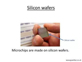
Technical issues for the future Silicon Wafers
160 likes | 531 Views
Technical issues for the future Silicon Wafers. *Kiyoshi Takada: Shin-Etsu Handotai Co., Ltd. (a former SSi General Manager) Masato Imai: Komatsu Electronic Metals Co., Ltd. (a former SSi Epitaxial Dept. Manager) Nobuyuki Hayashi: Sumitomo Mitsubishi Silicon Corp.

Technical issues for the future Silicon Wafers
E N D
Presentation Transcript
Technical issues for the future Silicon Wafers *Kiyoshi Takada: Shin-Etsu Handotai Co., Ltd. (a former SSi General Manager) Masato Imai: Komatsu Electronic Metals Co., Ltd. (a former SSi Epitaxial Dept. Manager) Nobuyuki Hayashi: Sumitomo Mitsubishi Silicon Corp. (SSi Administration Dept., General Manager) ITWG
Contents of presentation Q1. Why was the SSi consortium formed? Why was 400mm studied? Q2. What have been the SSi main technical success? Q3. How is the intellectual property rights performance going on? Q4. What are the key points for sending Technical Information to the Next Wafer Diameter? ITWG
SSi Q1. Why was the SSi consortium formed ? S = Super = Super Heavy and Large + Si = Silicon itself ITWG
(Quotation from the regime of SELETE at 1996) Q1. Why was 400mm studied? At the SSi establishment, it was a general agreement in the semiconductor industry that the next generation of 300mm was 400mm. ITWG
Q2. What have been the SSi main technical success? A2. 1) Monster CZ crystal pulling furnace by SSi original design. (Verification of “Maruyama Patent”, Cusp typed MCZ, etc.) 2) Wafer shaping process by SSi original Grinding Machines. (High flatness grinding technology in the lapping-less and etching-less process) 3) Low temperature Epitaxial growth by SSi original design. (Highly uniform growth of the super thin layer) ITWG
World largest CZ crystal pulling furnace • Furnace • Height: 12 m • Weight: 36 ton • Hot zone: 40 inch • Cusp-type super conductive magnet • Crystal • Diameter: 400 mm • Weight: over 400 kg • Body length: over 1m ITWG
Crystal Supporting System Schematic drawing of built-in system in SSi furnace M. Maruyama: Patent No. 1851653 ITWG
The world’s first Si single crystal weighing more than 400Kg in a 400mm diameter 400mm Si single crystal, which has a straight length of 110cm and a total weight of 411kg, is shown in contrast with normal 200mm crystal. ITWG
Four Trigonal Braces Top column Deionized water type hydraulic grinding spindle Twin double V guide ways Grinding wheel Trigonal Prism type Pentahedral Structure Base column Saddle Silicon wafer *Bed and base columns are cast as one component Deionized water type Linear actuator Bed Simplified wafer shaping process by Grinding Technology Schematic view of Ductile Mode Double Disk Grinding (DDG) Machine for Super-Large and Super-Flat Silicon wafer. ITWG
300 nm SEM photograph of cutting chip By the extremely high stiffness , motion accuracy, feeding resolution and fine mesh grinding wheel, a portion of Ductile-mode grinding was searched. ITWG
Q3. How is the intellectual property rights performance going on? A3. Among the many patents of SSi, the basic patents of Epi reactor are licensed to Tera Semicon (Korea). ITWG
Results of 400mm epitaxial wafers Note that the thickness distributions change drastically depending on the gas flow rate adjustment of each inlet nozzle. Thickness uniformity commensurate with industrial levels has been achieved. The transition width of 0.1mm is a very steep one compared to that of approximately 0.5mm for wafers grown by conventional SiHCl3 process. ITWG
Field Technological Issues Remarks Crystal Growth Standardization of Numerical Simulation and Thermal Properties. Δ ~ Χ Furnace system concept including MCZ, Crystal Suspending system, Larger Quartz Crucible, Safety system, etc. Ο Wafer Shaping Simplified Wafer Shaping process by Grinding Technologies with Ductile -mode. Ο ~ Δ High purity cleaning technology. Χ Low Temperature Epitaxial Growth Technology. Epitaxial Growth Ο ~ Δ Ο Epitaxial Furnace Design with the intention of Cost reduction. Metrology Defect & Particle Detection Technology. Χ Nano-Metrology System measuring the price detection of wafer shape. Ο ΟSSi information will be much effective. Δ Some of SSi information will be suggestive. ΧNew technology should be searched. Remarks: Q4. What are the key points for sending Technical Information to the Next Wafer Diameter ? A4. ITWG
Commercial Viability for Next Diameter crystal growth is questionable 1) Additional technologies such as Monster Puller installation with MCZ, giant Quartz Crucible, Suspending System,Remote Control, etc. will be needed. ⇒Higher cost 2) Productivity together with slower growth rate will drastically fall down. ⇒ Higher cost 3) Unusable Si materials such as shoulder, tail, residue, etc. will increase. φ400mm φ200mm ⇒Higher cost Weight loss >30% 10% ITWG
Concluding Remarks • SSi’s activity was a milestone to adapt our concept and/or strategy to the new circumstance. • SSi patents and know-how would be promised to improve the 300mm Si production and to the next generation wafer. • However, the fulfillment of the next wafer would be questionable without Devices, Equipment, Materials and Wafer each makers’ concrete cooperation and appropriate sharing of monster investment in advance. ITWG