Download

1 / 19
290 likes | 649 Views
Design and characterization of AlGaInAs quantum-well lasers. Academic advisor ︰ 郭艷光 教授 Reporter ︰ 謝尚衛 Number ︰ 92252005 Date ︰ 2003/1/6. Introduction.

E N D
Design and characterization of AlGaInAs quantum-well lasers Academic advisor︰郭艷光 教授 Reporter︰謝尚衛 Number︰92252005 Date︰2003/1/6
Introduction • Optical-fiber dispersion and loss are minimal at wavelengths near 1.3 and 1.55 mm, so semiconductor lasers emitting at these wavelengths are important light sources for optical networks. • A goal for many applications is highly efficient uncooled semiconductor lasers, which can be achieved using AlxGayIn1-x-yAs–InP instead of the conventional In1-xGaxAsyP1-y–InP material system. [1]–[4] 彰化師範大學光電工程技術研究所 謝尚衛
Band offset ratio of AlxGayIn1-x-yAs material system • The band offset ratio of AlxGayIn1-x-yAs is 0.72 : 0.28. • The band offset ratio of In1-xGaxAsyP1-y is 0.4 : 0.6. • Conclusion: The reduced carrier leakage results from AlxGayIn1-x-yAs – InP having a larger conduction band offset at the heterojunctions compared to the smaller conduction band offset of In1-xGaxAsyP1-y–InP, and this is very significant to prevent carrier leakage at high temperatures. References: PHYSICALREVIEWB VOLUME 47, NUMBER 11 MARCH 1993 APPLIEDPHYSICS LETTERS VOLUME 72, NUMBER 17 APRIL 1998 IEEE JOURNAL OF QUANTUM ELECTRONICS, VOL. 38, NO. 9, SEPTEMBER 2002 彰化師範大學光電工程技術研究所 謝尚衛
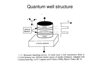
Energy diagram of a quantum well operating at 1.3 mm Reference:IEEE JOURNAL OF QUANTUM ELECTRONICS, MARCH 1995 彰化師範大學光電工程技術研究所 謝尚衛
Band-gap energy of AlGaInAs as a function of compositions. The figure shows that no bowing was observed. Reference: J. Appl. Phys. 63 (2), 15 January 1988 彰化師範大學光電工程技術研究所 謝尚衛
Schematic diagram of a 1.5 mm GaInAs/AlGaInAs quantum well laser diode primitively (1991). The active layer consisted of three Ga0.29In0.71As strained-layer quantum wells, each 25 Å thick, separated by 50-Å-thick Al0.2Ga0.28In0.52Asbarriers. Reference: Appl. Phys. Lett., Vol. 59, No. 11, 9 September 1991 彰化師範大學光電工程技術研究所 謝尚衛
L-I curve of the 1.5 mm GaInAs/AlGaInAs quantum well laser diode primitively (1991) in this experiment. The light output power versus injection current characteristics under pulsed operation is shown in left figure. Reference: Appl. Phys. Lett., Vol. 59, No. 11, 9 September 1991 彰化師範大學光電工程技術研究所 謝尚衛
Design of 1.3 mm AlGaInAs–InP multiple-quantum-well lasers recently(2001). This is a schematic representation of a ridge-waveguide laser. The active layer consisted of five Al0.161Ga0.102In0.737Asstrained-layer quantum wells, each 50 Å thick, separated by 100-Å-thick Al0.267Ga0.203In0.53Asbarriers. Reference: IEEE JOURNAL ON SELECTED TOPICS IN QUANTUM ELECTRONICS, VOL. 7, NO. 2, APRIL 2001 彰化師範大學光電工程技術研究所 謝尚衛
Index of refraction along the epitaxial structure. The epitaxial structure shown above is composed of five quantum wells, four barriers, two graded-index (GRIN) layers, inner cladding layers, transition GRIN layers, one p-spacer, etch stop, and outer cladding. 彰化師範大學光電工程技術研究所 謝尚衛
Energy gap ofAlxGayIn1-x-yAs The relation between energy gap and aluminum mole fraction for the AlGaInAs material system is summarized in this table. Reference: IEEE JOURNAL ON SELECTED TOPICS IN QUANTUM ELECTRONICS, VOL. 7, NO. 2, APRIL 2001 彰化師範大學光電工程技術研究所 謝尚衛
Threshold current as a function of cavity length for different operating temperatures. The relationship between the threshold current of the five-quantum-well structure and its cavity length for different temperatures is shown above. 彰化師範大學光電工程技術研究所 謝尚衛
Experimental light-current characteristics for the 1.3 mm AlGaInAs–InP laser. The ridge width, cavity length, and reflectivities are 5 mm, 250 mm, and 30%/70%, respectively. 彰化師範大學光電工程技術研究所 謝尚衛
Another special design of 1.3 mm AlGaInAs–InP multiple-quantum-well lasers (1998). This is a schematic conduction band diagrams of the three laser structures: (a) conventional step-index SCH, (b) SMQB, and (c) DMQB. Reference:APPLIED PHYSICS LETTERS VOLUME 72, NUMBER 17APRIL 1998 彰化師範大學光電工程技術研究所 謝尚衛
Multiquantum barrier (MQB) structure The slope efficiency and threshold current density of 1.3 mm AlGaInAs–InP lasers with AlInAs–AlGaInAs multiquantum barrier (MQB) are experimentally studied and compared with the conventional step- index separate confinement heterostructure (SCH) laser. With the MQBs at the guiding layers, the characteristictemperature can be improved as much as 10 K as compared with the conventional SCH laser. This is attributed to the suppression of electron and hole leakage currents. Reference:APPLIED PHYSICS LETTERS VOLUME 72, NUMBER 17APRIL 1998 彰化師範大學光電工程技術研究所 謝尚衛
Threshold current density as a function of temperature for the lasers with and without MQBs. Multiquantum barrier (MQB) structure has shown great potential on decreasing threshold current and raising characteristic temperature of quantum well lasers. 彰化師範大學光電工程技術研究所 謝尚衛
Comparison of the long-distance material systems Reference:APPLIED PHYSICS LETTERS VOLUME 79, NUMBER 19 NOVEMBER 2001 彰化師範大學光電工程技術研究所 謝尚衛
Conclusion • Low-cost, high-performance 1.3 and 1.55- mm-wavelength semiconductor lasers are important for optical interconnection. • And the new material systems such as AlGaInAs have been tried. • Because of the conduction band offset greater than 0.5, the electron leakage is reduced and the laser properties become better than those of the InGaAsP system. • In this winter vacation, I will make efforts in the AlGaInAs material system, and expect to obtain good results. 彰化師範大學光電工程技術研究所 謝尚衛
References [1] T. Higashi et al., “Observation of reduced nonradiative current in 1.3-m AlGaInAs-InP strained MQW lasers,” IEEE Photon. Technol. Lett., vol. 11, pp. 409–411, Apr. 1999. [2] M. Yamada et al., “High temperature characteristics of 1.3-m InAsPInAlGaAs ridge waveguide lasers,” IEEE Photon. Technol. Lett., vol. 11, pp. 164–166, Feb. 1999. [3] K. Takemasa et al., “1.3-m AlGaInAs buried-heterostructure lasers,” IEEE Photon. Technol. Lett., vol. 11, pp. 949–951, Aug. 1999. [4] C. E. Zah, R. Bhat, B. N. Pathak, F. Favire, W. Lin, M. C. Wang, N. C. Andreadakis, D. M. Hwang, M. A. Koza, T. P. Lee, Z. Wang, D. Darby, D. Flanders, and J. J. Hsieh, “High-performance uncooled 1.3- m Al Ga In As/InP strained-layer quantum-well lasers for subscriber loop applications,” IEEE J. Quantum Electron., vol. QE-30, pp. 511–521, 1994. 彰化師範大學光電工程技術研究所 謝尚衛
Thanks for your attention ! 彰化師範大學光電工程技術研究所 謝尚衛