Download
1 / 11
570 likes | 1.54k Views
6. Semiconductor quantum well. 6.1 Quantum confined structures 6.2 Growth and structure of semiconductor quantum wells 6.3 Electronic levels 6.4 Optical absorption and excitons 6.5 Optical emission 6.6 Intersubband transitions 6.7 Quantum dot. Single quantum well .

E N D
6 Semiconductorquantum well 6.1 Quantum confined structures 6.2 Growth and structure of semiconductor quantum wells 6.3 Electronic levels 6.4 Optical absorption and excitons 6.5 Optical emission 6.6 Intersubband transitions 6.7 Quantum dot
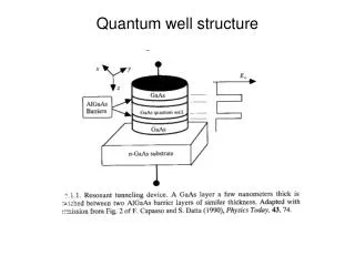
Single quantum well 6.1 Quantum confined structures Quantum confinement effect: pX h / x . Econfinement = (pX )2/ 2m h2 / 2m(x)2 If Econfinement > 1/ (2 kBT), that is x deB Quantum size effects will be important. x 5 nm (me*= 0.1 m0, electrons in semi- conductor at RT) Threebasic types of quantum confined structure A single GaAs/AlGaAs quantum well. It is formed in the thin GaAs layer sandwiched between AlGaAs layers which have a large band gap. d is chosen so that the motion of the electrons in the GaAs layer is quantized in z direction. The lower figure shows the spatial variation of the conduction band (C.B) and the valence band (V.B) that corresponds to the change of composition. The band gap of AlGaAs is larger. The electrons and holes in GaAs layer are trapped by the potential barriers at each side by the discontinuity in the C.B and V.B. These barriers quantize the states in the z direction, but the motion in x, y plane is still free. 6.2 Growth and structure of semiconductor quantum wells heterostructure made by epitaxial growth technique: MBE and MOCVD
6.2 Growth and structure of semiconductor quantum wells 6.3 Electronic levels 6.3.1 Separation of the variables Wavefunction: The total energy: MQW or superlattice The x, y plane motion is free, the wave function of plane waves: where A is the normalization area. The kinetic energy: The total energy: 6.3.3 Infinite potential wells: GaAs / AlGaAs multiple quantum well (MQW) or superlattice The distinction between them depends on the thickness b of the barrier separating the quantum wells. MQWs have lager b value, the individual quantum wells are isolated from each other. Superlattices, by contrast, have much thinner barriers, the quantum wells are thus coupled by tunnelling through the barrier, and new extended states are formed in the z direction. E1= 38 mV; E2= 150 mV; kBT=25 mV; m* =0.1 m0.
6.3.3 Finite potential wells: Wave function in the well: Although the infinite well model overestimates the confinement energies, it is a useful starting point for the discussion because of its simplicity. Note that the separation of the first two electron level is more than three times the thermal energy at RT, where kBT 25 meV. where For the finite potential barrier, the electrons and holes tunnel into the barriers, the Schrodinger equation in the barrier regions:
6.4 Optical absorption and excitons 6.4.1 Selection rules Photons incident on a quantum well with light propagating in the z direction. The electrons from an initial state i at energy Ei in the valence band are excited to a finial state f at energy Ef in the conduction band. Conservation of energy requires that Ef = (Ei + h). Interband optical transitions in a quantum well. The figure shows a transition from an n=1 hole level to an n=1 electron level, and from an n=2 hole level to an n =2 electron level. Fermi’s golden rule of the transition: There are three factors in these two wave functions: 1. Conservation of momentum in the transition: kxy = k’xy ; 2-3. M = MCV Mnn’ MCV is the valence- conduction band dipole momentum; The matrix element (selection rule): The polarization vector of the light is in the x, y plane, thus we have: f x i = f y i f z i ) Considering a general transition from the nth hole state to the n’th electron state, we can write the initial and final quantum well wave functions in Bloch function form: Mnn’ is the electron-hole overlap.
6.4.1 Selection rules Mnn’= 1 if n = n’, Mnn’ = 0 otherwise. Selection rules for infinite quantum well: n = 0 In finite quantum wells the electron and hole wave functions with differing quantum numbers are not necessarily orthogonal to each other because of the differing decay constant in the barrier regions. This means that there are small departures from the selection rule of a infinite quantum well. However these non-zero transitions are usually weak, and are strictly forbidden if n is an odd number, because the overlap of states with opposite parities is zero. Interband optical transition in a quantum well at finite kxy. 6.4.2 Two-dimensional absorption The threshold (absorption edge ): h = Eg + Ehh1 + Ee1, (Shifted by (Ehh1 + Ee1) compared to the bulk) The frequency of absorption: The absorption coefficient for an infinite quantum well of width d The threshold energy for the nth transition: The joint density of state (step-like)
6.4.3 Experimental data 6.4.4 Excitons in quantum wells Absorption coefficient of a 40 period GaAs/AlAs MQW structure with 7.6 nm quantum wells at 6 K. The steps in the spectrum are due to the n = 0 transition. The first of these occurs for the n = 1 heavy hole transition at 1.59 eV. This is closely followed by the step due to the n = 1 light hole transition at 1.61eV. The steps at the band edge are followed by a flat spectrum up to 1.74 e. At 1.77 eV there is a further step due to the onset of the n = 2 heavy hole transition, then n = 3 at 2.03 eV…. The two weak peaks identified by arrows are caused by parity-conserving n 0 transitions. The one at 1.69 eV is the hh3 -> e1, while that at 1.94 eV is the hh1-> e3 transition. RT absorption spectrum of a GaAs/ Al0.28Ga0.72As MQW structure containing 77 GaAs quantum wells of width 10 nm. The spectrum of GaAs at the same temperature is shown for comparison. Detailed analysis reveals that the binding energies of the quantum well excitons are about 10 me, higher than the value of 4.2 meV in bulk GaAs. The enhancement is a consequence of the quantum confinement of the electrons and holes in the QW. The excitons are still stable at RT in the QW. The bulk sample merely shows a weak shoulder at band edge, but the MQW shows strong peaks for both the heavy and the light hole excitons. The lifting of the degeneracy originates from the different effective masses of the heavy and light holes and the lower symmetry of the QW sample.
6.5 Optical emission Zn0.8Cd0.2Se/ZnSe is a II-VI alloy semiconductor with a direct band gap of 2.55 eV at 10K, and ZnSe has a band gap of 2.82 eV • The use of quantum well structure in EL devices is their main commercial application: • A greater range of emission wavelength; • An enhancement of device efficiency. • Emission spectrum for bulk semiconductor: Emission spectrum for QW: 1. The (hv -Eg)1/2 factor from will be replaced by the unit step function derived from the 2-D density of states; 2. The peak at energy: hv=Eg+Ehh1+Ee1, is shifted by the quantum confinement of the electrons and holes to higher energy; 3. spectral width kBT. Emission spectrum of a 2.5 nm Zn0.8Cd0.2Se/ZnSe quantum well at 10 K and RT. The spectrum at 10 K peaks at 2.64 eV(470 nm) and has a full width at half maximum of 16 meV. The emission energy is about 0.1 eV larger than the band gap of the bulk material, and the line width is limited by the inevitable fluctuations in the well width that occur during the epitaxial growth. At RT the peak has shifted to 2.55 eV(486 nm) with the broadened line width about 2.55 meV(~ 2kBT) . • Main advantages: • the wavelength of light emitting is tunable by choice of the • well width; • the emission probability is higher, and the radiative lifetime • is shorter, the radiative recombination wins out over • competing non-radiative decay mechanisms; • the thickness of QW is well below the critical thickness for • dislocation formation in non – lattice - matched epitaxial • layers.
6.7 Quantum dots (QD) 6.6 Intersubband transitions The electrons and holes are excited between the levels (or ‘subband’) within the conduction and valence band. A quantum dot structure may be considered as a 3-D quantum well, with no degrees of freedom at all and with quantized levels for all three directions of motion. For a rectangular dot with dimensions (dx, dy,dz), the energy levels ( the infinite barriers assumed in all three directions): The energy spectrum is completely discrete. The energy levels is tunable by altering the size of the QD. The intersubband transition corresponds to an infrared wavelength. Selection rule on n = ( n -- n’ ) is that n must be an odd number. Quantum cascade laser …… Variation of the electron density of states with dimensionality. The dashed line shows the (E–Eg )1/2 dependence of the bulk material. The thin solid line corresponds to a quantum well with the characteristic step-like density of states of 2-D materials. The thick solid line shows the density of states with a series of delta functions at the energies described by above eqn for the 0-D quantum dot.
6.7.2 Self-organized III-V quantum dots 6.7 Quantum dots (QD) 6.71 Semiconductor doped glasses II-VI semiconductor such as CdS, CdSe, ZnS and ZnSe are introduced into the glass during the melt process, forming very small microcrystals with the glass matrix. It is possible to make quantum dots with good size uniformity. The dot are typically formed when we try to grow layer of InAs on a GaAs substrate. There is a large mismatch between the lattice constant of the epitaxial layer and the substrate. In the right conditions, it is energetically advantageous for the INAs to form small clusters rather than a uniformly strained layer. The surface physics determines that the dimensions of these clusters is of order 10 nm, which provides excellent quantum confinement of the electrons and holes in all three directions. Absorption spectra of glasses with CdS microcrystals of varying at 4.2 K. Spectra are shown for four different sizes of the microcrystals. Quantum size effects are expected when the d of the crystal is less than 3.5 nm. The sample with d = 33 nm effectively represents the properties of bulk CdS (band edge occurs at 2.58 eV). The others show an increasing shift of the absorption edge to higher energy with decreasing dot size (a shift of over 0.5 eV for the sample with d = 1.2 nm). The spectra also show a broad peak at the edge which is caused by the enhanced excitonic effects.
4. The matrix element for an intersubband transition between the nth and n’th subbands of a quantum well is given by: i) By considering the parity of the states, prove that n= n - n’ must be an odd number. ii) Compare the relative strengths of the 1-> 2 and 1-> 4 transitions in a 20 nm GaAs quantum well with infinite barriers. What is the wavelength of the 1-> 2 transition ? (me*=0.067m0) Exercises: 1. A particle of mass m* is confined to move in a quantum well with infinite barriers of width d. Show that the energy separation of the first two levels is equal to (½) kBT when d is equal to d = ( 3h2/4m* kBT)1/2. Evaluate d for electrons of effective mass m0 and 0. 1m0 at 300K. Hence show that this value of d is smaller than the value of x given in eqnx ~ by a factor of 32. 2. Estimate the difference in the wavelength of the absorption edge of a 20 nm GaAs quantum well and bulk GaAs at 300 K.(Table C.2) 3. Estimate the emission wavelength of a 15 nm GaAs quantum well laser at 300K.(Table C.2)