Download
1 / 11
120 likes | 349 Views
Quantum Well Applications. ECE 4611 – Semiconductors Presented by: Joshua MacDonald & Joel Peterson 29 APRIL 2013. Abstract.

E N D
Quantum Well Applications ECE 4611 – Semiconductors Presented by: Joshua MacDonald & Joel Peterson 29 APRIL 2013
Abstract In this powerpoint, we present some modern-day technical applications of quantum well technology. The small wavelengths made possible by the well dimensions, which are generally in the scale of nanometers, are useful in optics for diode lasers, in measuring devices for IR photo detectors, and in micro-electronics for high electron mobility transistor devices. Many of these devices group or layer quantum wells to improve output or performance.
Administrative • Outline • Review • General Application • Applied • Optics, lasers and detectors • High speed electronics, transistors • Key-points
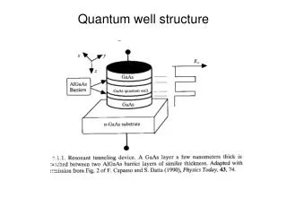
Review (Properties) • Two-dimensional (mostly) devices • Discrete energy values
Applications • Generalities • Quantum dimensions make very small λ possible. • Quantum construction means less material, higher speeds.
Optics • Diode lasers • Measuring devices • Communications
Lasers • Quantum Well and Quantum Cascade Lasers • Device geometry(well) is more important than band structure of the semiconductor. • Sometimes layered. IV curve of a QCL (ALPSLASERS QCL)
Measuring Devices • Quantum Well IR Photo detector • Arrays of QW’s “tuned” to a λ. • Often used in imaging (Medical, Military)
Micro-Electronic • High Electron Mobility Transistor devices • Single and Multi Quantum Well structures • Often employ Quantum Hall Effect
Key Points • Optical applications exploit low λpossible with QW’s • Detection devices also employ QW’s because of the lower λ’s detectable • HEMT’s speed and performance enabled by QW(Quantum Hall Effect) • Devices often layer or group QW’s to improve characteristics • There are many proprietary design/material combinations
References • http://www.nextnano.de/ (3d device modeling software) (well structure graphic) • QCL http://www.alpeslasers.ch/?a=36,37 • QWIP http://www.3-5lab.fr/Scope4-2.htm