Download

1 / 22
230 likes | 651 Views
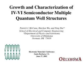
Growth and Characterization of IV-VI Semiconductor Multiple Quantum Well Structures . Patrick J. McCann, Huizhen Wu, and Ning Dai* School of Electrical and Computer Engineering *Department of Physics and Astronomy University of Oklahoma Norman, OK 73019 Electronic Materials Conference

E N D
Growth and Characterization of IV-VI Semiconductor Multiple Quantum Well Structures Patrick J. McCann, Huizhen Wu, and Ning Dai* School of Electrical and Computer Engineering *Department of Physics and Astronomy University of Oklahoma Norman, OK 73019 Electronic Materials Conference Santa Barbara, CA June 27, 2002
Outline • IV-VI Semiconductors • Biomedical Applications • MBE Growth and Characterization • Square and Parabolic MQWs • Summary
IV-VI Semiconductors (Pb-Salts) • Unique Features • High Dielectric Constants Defect Screening • Can be Grown on Silicon Low Cost, Integration Possibilities • Symmetric Band Structure High Electron and Hole Mobilities • Applications • Thermoelectric Coolers (Low Lattice Thermal Conductivity) • Infrared Detectors (Silicon Integration Possible) • Spintronics (Quantum Dots with Magnetic Impurities) • Tunable Mid-IR Lasers (Medical Diagnostics, etc.)
~~ ~~ ~~ IV-VI Laser Materials Pb1-xSnxSe PbSrSe p-type Double Heterostructure Laser PbSe n-type PbSrSe n-type PbSe Substrate
Heat Sink Heat Sink Breath Analysis with IV-VI Lasers IV-VI Laser
Asthma Diagnosis Laser Focus World, June 2002, P. 22 Roller et al., Optics Letters27, 107 (2002). • High exhaled NO indicates airway inflammation. • People with asthma suffer from chronic airway inflammation. • Quantum cascade mid-IR lasers have not been able to do such measurements even though several attempts have been made.
IV-VI Epitaxial Layers • High quality layers can be grown on silicon • McCann et al., Journal of Crystal Growth175/176, 1057 (1997). • Strecker et al., Journal of Electronic Materials26, 444 (1997). • Room temperature cw photoluminescence • McCann et al., Applied Physics Letters75, 3608 (1999). • McAlister et al., Journal of Applied Physics 89, 3514 (2001). • Optical devices on silicon • Through-the-substrate inter-chip optical interconnects (PC Magazine, January 21, 2002). • Modulators for free-space optical communication. • Infrared imaging arrays.
In Situ RHEED MBE Growth on Silicon and BaF2 IV-VI MBE Chamber at OU Sources: PbSe, Sr, Se, PbTe, BaF2, CaF2, Ag, Bi2Se3 Si(111) (77) after oxide desorption BaF2 (111) substrate (11) at 500 °C • SiO2 desorption at 700°C allows epitaxial growth of nearly lattice-matched CaF2 on Si • CaF2 growth on Si is layer-by-layer • BaF2 growth on CaF2 is layer-by-layer • PbSrSe growth on low surface energy BaF2 is initially 3D (island) • PbSrSe layer eventually becomes 2D after growth of more than 1 µm After growth of 6 Å of PbSrSe on BaF2 After growth of 2 nm CaF2 After growth of 600 nm BaF2 After growth of 3 µm of PbSrSe on BaF2
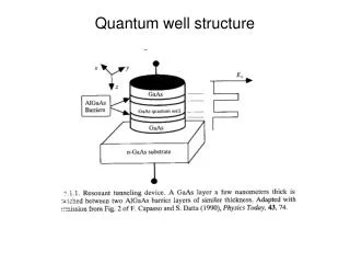
Si Substrate BaF2 Substrate PbSe/PbSrSe MQWs HRXRD 4 nm to 100 nm • MQWs on Si have high crystalline quality • MQWs on BaF2 substrates have higher crystalline quality due to better thermal expansion match
BaF2 Substrates Photoluminescence Near-IR (~980 nm) cw diode laser pumping (low intensity, ~250 mW) • Strong Quantum Size Effect • Strong CW Emission at 55°C • Interference Fringes Dominate Spectra • Spacings depend on index of refraction and epilayer thickness • Strong optical resonance indicates stimulated emission processes
Si Substrate Mid-IR Emitter on Silicon Si Substrate IV-VI MQW Near-IR (~980 nm) cw diode laser (~250 mW) Emission through Silicon Substrate – Promising optical interconnect architecture
Less epilayer heating with higher thermal conductivity silicon substrates BaF2 Substrate Silicon Substrates Optical Heating of Epilayers H. Z. Wu et al., J. Vac. Sci. and Technol. B 19, 1447(2001). InGaAs (972 nm) diode laser pump current
20.6 nm 4 nm to 100 nm IR Transmission LQW=20.6 nm Differential Transmission Fourier Transform Infrared Spectroscopy – Subtract transmission spectra collected at two different temperatures – Peaks yield interband transition energies H. Z. Wu et al., Applied Physics Letters78, 2199 (2001).
Oblique Oblique Normal Oblique mOe = 0.0475 mNe = 0.0788 mNh = 0.0764 mOh = 0.0408 Normal Oblique (3-Fold Degenerate) Removal of L-Valley Degeneracy • Direct gap is at the L-point in k-space • Four Equivalent L-valleys • Symmetric conduction and valence bands • Potential variation in [111] direction • One L-valley is normal to the (111) plane in k-space • Three L-valleys are at oblique angles • Two different effective masses for electrons (and holes) in the PbSe MQWs
(1-1)O (1-1)O (1-1)N Eg (PbSe) = 150 meV (4K) (1-1)O Interband Transitions
Energy Levels Oblique Normal
PL Emission Oblique Valleys Density of States • Lowest energy level has a low density of states • Lower threshold for population inversion • Stimulated emission at low excitation rates • Four-level laser design
Lasing Thresholds • IV-VI Mid-IR VCSELs • Bulk Active Region • Optical pumping threshold: 69 kW/cm2 • Z. Shi et al., Appl. Phys. Lett., 76, 3688 (2000) • MQW Active Region • Optical pumping threshold: 10.5 kW/cm2 • C. L. Felix et al., Appl. Phys. Lett.78, 3770 (2001)
Expect Evenly-Spaced Harmonic Oscillator Eigenvalues Parabolic MQWs
Parabolic MQW Analysis Equally Spaced Energy Levels (Harmonic Oscillator) • Measured bandgaps in strained PbSe (caused by lattice mismatch with PbSrSe) compared to 77 K bandgap for bulk PbSe allows determination of deformation potentials: Dd = 6.1 eV and Du = -1.3 eV. • Energies for the higher confined states in 100 nm sample allows determination of band non-parabolicity parameters: c = v = 1.910-15 cm2
Summary • IV-VI semiconductors are versatile materials for a variety of applications. • A mid-IR laser spectroscopy application for asthma diagnosis has been developed. • PbSe-based MQW structures have attractive properties for improved mid-IR laser technology. • L-valley degeneracy removal. • Energy level structure in MQWs on (111)-oriented substrates enables low population inversion thresholds.