Download
1 / 20
200 likes | 217 Views
Explore the features and performance of the FSSR2 chip designed for the BTeV Forward Silicon Tracker. Learn about its architecture, data output, noise behavior, and potential applications.

E N D
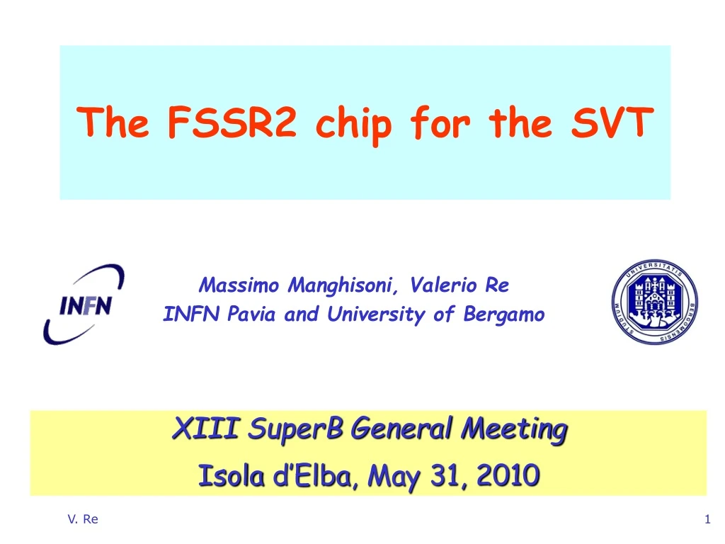
The FSSR2 chip for the SVT Massimo Manghisoni, Valerio Re INFN Pavia and University of Bergamo XIII SuperB General Meeting Isolad’Elba, May 31, 2010
FSSR2 • Fast, data driven readout architecture, with no analog storage, with large output bandwidth • FSSR2, designed for the BTeV Forward Silicon Tracker (Pavia/Bergamo-Fermilab), has the right features: • Mixed-signal integrated circuit for the readout of silicon strip detectors (selectable shaper peaking time: 65-85-100-125 ns) • TSMC 0.25 µm CMOS tech. with enclosed NMOS Rad. Hard • 128 analog channels, sparsified digital output with address, timestamp, and pulse height information for all hits • Architecture designed to run with 132 ns bunch crossing (timestamp granularity = BCO clock = 7.6 MHz), readout clock @ 70 MHz • 840 Mb/s output data rate • For more details on FSSR2 see for example: • V. Re et al., “FSSR2, a Self-Triggered Low Noise Readout Chip for Silicon Strip Detectors”, 2005 IEEE Nuclear Science Symposium Conference Record • V. Re: “First prototype of a silicon microstrip detector with the data-driven readout chip FSSR2 for a tracking-based trigger system” , presented @ 10th Pisa Meeting on Advanced Detectors, La Biodola (Isola d’Elba), May 21 – 27, 2006 SuperB Workshop 02/12/2009
FSSR2 block diagram • The FSSR2 chip architecture is virtually identical to that of FPIX2. • Each strip is treated as one pixel cell (Pseudo-Pixel architecture)[*] • It can be described as including four sections • FSSR2 Core • 128 analog channels • 16 sets of logic, each handling 8 channels (EOS Logic) • Core logic with BCO counter (time stamp) • Programming Interface(slow control) • Programmable registers • Data Output Interface 128 channels of analog circuits End-Of-Set Logic 16 Sets of logic each handling 8 analog channels CORE Core Logic Clock Control Logic Next Block Word PROGRAMMABLE REGISTERS DACs DATA OUTPUT INTERFACE Word Serializer PROGRAMMING INTERFACE Steering Logic FSSR clk MCA/MCB I/O High Speed out [*] PreFPIX2: core architecture and resultsHoff, J.R.; Mekkaoui, A.; Christian, D.C.; Zimmerman, S.; Cancelo, G.; Kasper, P.; Yarema, R.;Nuclear Science, IEEE Transactions on, Volume 48, Issue 3, Part 1, June 2001 Page(s):485 - 492
Preamplifier Programmable Gain To 3-bit Flash ADC Cf1 Programmable Baseline Restorer Analog channel (evolution of AToM) Cf Hit/NoHit Discriminator Bias + Threshold circuit Shaper Gf Comparator CD Kill Single-ended/ Differential conversion - BLR Vth CR-(RC)2 - + CAC Cinj Test Input (from Internal Pulser) Programmable Peaking time (65 ns - 125 ns) Threshold DAC (chip wide)
FSSR2 and SuperB SVT • FSSR2 has been evaluated for a possible use in: • Layer 0: striplets, low capacitance, high background rate • Outer layers: long strips (higher capacitance and strip resistance, smaller background) • FSSR2 has a very good noise behavior in a wide range of detector capacitances SuperB Workshop 02/12/2009
Layer 0 S/N with FSSR2 FSSR2 noise vs det Capacitance • Assume noise performance as measured in FSSR2: • ENC=a+b*CD • a=240 e- , b=35 e-/pF • Serie resistance increases by ~ 14% the slope b: Rs = Lfanout *2/cm + Ldet*20/cm=55 e_n=4kT Rs/3 Equivalent Noise Charge = 600 e- CD = 9pF • Signal = 16000 e- (Si 200 um thick) • S/N = 26( ~ 24 including 300 e- thr. dispersion added to noise in quadrature) SuperB Det. Meeting 12/12/2006
Noise forecast for SVT external layers From L. Bosisioslides, 17/9/09, SuperB SVT meeting: Worst case: SVT externallayers, Phi-side layer5. Strips 37 cm long. C = 1.5 pF/cm R = 10 W/cm CD = 55 pF, RS = 370 W Expected ENC = 1400 e rms at tP = 125 ns and no BLR (best case for FSSR2, may be unnecessary if occupancy is low), neglecting noise from series strip resistance and parallel noise (detector leakage and bias resistor) SuperB Workshop 02/12/2009
thermal noise of the distributed resistance RS thermal noise of preamplifier input NMOS 1/f noise of preamplifier input NMOS Parallel noise from detector leakage current and bias resistor ENC equation SuperB Workshop 02/12/2009
Noise by strip series resistance At the FSSR2 peaking times (e.g. tP = 125 ns) and input device parameters (e.g., ID = 500 mA) (as is), noise from the series strip resistance is by far the dominant contribution FSSR2 as is No gain in S/N by acting on the FSSR2 preamplifier It will be no different with another chip FSSR2 as is SuperB Workshop 02/12/2009
Increase peaking time Keep ID = 500 mA, W/L = 1500/0.45 (as is in FSSR2), increase tP large gain, possible upper limit set by occupancy (parallel and 1/f noise do not seem be a severe limitation) FSSR2 as is S/N = 26 at tP = 1 ms (no BLR) S/N = 20 at tP = 400 ns (no BLR) SuperB Workshop 02/12/2009
The FSSR2 Verilog Model 128 “Strips” Ordered by BCO 128 “Strips” With timing info 1,2,4, or 6 serial lines + Output Clk SiliconStrip Det. Model Data Outputs MonteCarloData FSSR Model DAQModel Strip Inputs Report Control Inputs daq.v daq.v FSSR2.v stripBlocks.v stripCell.v stripEOC.v stripCore.v stripDataInt.v stripProgInt.v stripConstants.v fStripDat.out Silhits_2int.dat FSSR Clk, Master Clocks, Serial In, Out and Ctrl RecordedEvents, Misses, Matches List Of Originals fStripOut.out fStripMatch.out fStripMis.out fStripMisO.out fStripScratch.out fStripIn.out FSSR Status Report: Completion of the Functional Design PhaseHoff, J.R.; Mekkaoui, A.; Yarema, R.
Occupancy In Layer 1 we can expect a FSSR2 event rate up to about 500 kHz on each strip: Assuming bkg rate of 1MHz/cm2, 2 hit/track, 10.7cm strip length, 50μm pitch, including a safety factor 5 Event Rate = 535 kHz 900 kHz in Layer 0 At 30 MHz FSSR clock, the average occupancy in an FSSR clock period is 1.8% (with a factor of 5 safety factor) 3 % in Layer 0 In the following the chip efficiency will be shown as a function of the Event Rate
Monte Carlo Data file 128 columns (one for each strip) 0000000000000 0000000000000 0000001000000 000001000 000000000 010000000 • 1 Row = 1 Time Slice • 1 Time Slice = 1 FSSR Clk Period ………. # rows (one for each time slice) …… …… 000000000 000000000 000010000 0000100000000 0000000000011 0000000000000 ………. # events Occupancy [%] = · 100 # rows · 128 # events · FSSR clock frequency Event Rate [Hz] = # rows · 128
Efficiency vs FSSR Clock • Efficiency increases at FSSR clock frequency higher than 7.5 MHz • No big difference between 22 MHz and 30 MHz • No detected events at FSSR clock higher than 30 MHz • Even at 30 MHz of FSSR Clock we have a very low efficiency at the expected Event Rate
Efficiency vs Master Clock • Efficiency increases with the increase of the Master Clock. • At the expected Event Rate the FSSR efficiency falls down even at the highest MClk frequency of 90 MHz.
Conclusions (I) According to Verilog simulation results the best performances of the FSSR2 chip can be obtained in the following configuration: The model seems to fail at the foreseen Event Rate
Conclusions (II) Occupancy vs efficiency: Further Verilog tests are being carried out to understand the steep decrease in efficiency Given the large background, we may consider using a triggered architecture instead of a data push one The chip for the ATLAS-SCT (80 um pitch) is a good example of how such an architecture can deal with a 2% occupancy (25 ns time slice) SuperB Workshop 02/12/2009
Conclusions (III) Noise in outerlayers (long strips): The mainnoisecontribution (thermalnoise in strip distributedresistance) doesnotdepend on the readout chip Wemayconsiderusing a triggeredarchitecture in outerlayerstoo, whichmightallowfor a long enoughshapingtimetoachieveanadequate S/N SuperB Workshop 02/12/2009
Backup SuperB Workshop 02/12/2009
Occupancy vs FSSR Clock • 1.3 % • 0.8 % • 0.4 % • Occupancy @ FSSR clk = BCO • 0.3 % • 0.2 % • 0.1 % • Occupancy @ FSSR clk = 4BCO