Download
1 / 13
130 likes | 230 Views
Explore the advanced features and specifications of the STAR-SVT device, offering precise bi-directional drift measurement. Learn about its design and performance in detecting particles accurately.

E N D
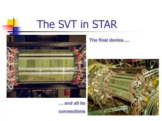
The SVT in STAR The final device…. … and all its connections
STAR-SVT characteristics • 216 wafers (bi-directional drift) = 432 hybrids • 3 barrels, r = 5, 10, 15 cm, 103,680 channels, 13,271,040 pixels • 6 by 6 cm active area = max. 3 cm drift, 3 mm (inactive) guard area • max. HV = 1500 V, max. drift time = 5 ms, (TPC drift time = 50 ms) • anode pitch = 250 mm, cathode pitch = 150 mm • SVT cost: $7M for 0.7m2 of silicon • Radiation length: 1.4% per layer • 0.3% silicon, 0.5% FEE (Front End Electronics), • 0.6% cooling and support. Beryllium support structure. • FEE placed beside wafers. Water cooling. R. Bellwied, Snowmass 2001
Wafers: Performance • Unambiguous XY coordinates • 250 mm x-pitch, 20 ns y-time, ENC = 500e, vdrift = 6.5mm/ns • Along X (anodes) determined by anode pitch and noise. Typically less than 10mm. • Along Y (drift) determined by time bucket width, noise, and homogeneity of implanted resistors. Typically less than 20mm. R. Bellwied, Snowmass 2001
Typical SDD Resolution R. Bellwied, Snowmass 2001
Wafers: B and T dependence • Used at B=6T. B fields parallel to drift increase the resistance and slow the drift velocity. • The detectors work well up to 50oC but are also very T-dependent. T-variations of 0.10C cause a 10% drift velocity variation • Detectors are operated at room temperature in STAR. • We monitor these effect via MOS charge injectors R. Bellwied, Snowmass 2001
Present status of technology STAR • 4in. NTD material, 3 kWcm, 280 mm thick, 6.3 by 6.3 cm area • 250 mm readout pitch, 61,440 pixels per detector • SINTEF produced 250 good wafers (70% yield) ALICE • 6in. NTD material, 2 kWcm, 280 mm thick, 280 mm pitch • CANBERRA produced around 100 prototypes, good yield Future • 6in. NTD, 150 micron thick, any pitch between 200-400 mm • 10 by 10 cm wafer R. Bellwied,Snowmass 2001
Silicon detector option for LCD(small detector, high field B=5T) Forward tracker: Silicon Strip Five disks uniformly spaced in z Radiation length / layer = 1.0 % Double-sided with 90 degree stereo, sigma = 7mm Inner radii Outer radii Z position ----------- ----------- ---------- 4.0 cm 20.50 cm 27.1 cm 7.9 cm 46.75 cm 62.1 cm 11.7 cm 73.00 cm 97.1 cm 15.6 cm 99.25 cm 132.1 cm 19.5 cm 125.50 cm 167.1 cm Vertex detector:CCD 5 layers uniformly spaced (r = 1.2 cm to 6.0 cm) Half-length of layer 1 = 2.5 cm Half-length of layers 2-5 = 12.5 cm sigma_rphi = sigma_rz = 5 microns Radiation length / layer = 0.1 % Central tracker: Silicon Drift DetectorsFive layers Radiation length / layer = 0.5 % sigma_rphi = 7 mm, sigma_rz = 10 mm Layer Radii Half-lengths ----------- ------------ 20.00 cm 26.67 cm 46.25 cm 61.67 cm 72.50 cm 96.67 cm 98.75 cm 131.67 cm 125.00 cm 166.67 cm 56 m2 Silicon Wafer size: 10 by 10 cm # of Wafers: 6000 (incl. spares) # of Channels: 4,404,480 channels (260 mm pitch)
Mature technology. <10 micron resolution achievable with $’s and R&D. Easy along one axis (anodes). <0.5% radiation length/layer achievable if FEE moved to edges. Low number of channels translates to low cost silicon detectors with good resolution. Detector could be operated with air cooling at room temperature Silicon Drift Detector Features R. Bellwied, Snowmass 2001
Improve position resolution to 5mm Decrease anode pitch from 250 to 100mm. Stiffen resistor chain and drift faster. Improve radiation length Reduce wafer thickness from 300mm to 150mm Move FEE to edges or change from hybrid to SVX Air cooling vs. water cooling Use 6in instead of 4in Silicon wafers to reduce #channels. More extensive radiation damage studies. Detectors/FEE can withstand around 100 krad (g,n) PASA is BIPOLAR (intrinsically rad. hard.) SCA can be produced in rad. hard process. R&D for Large Tracker Application R. Bellwied, Snowmass 2001
Simulation Studies • Momentum resolution • Present: 20 mm pos.res., 1.5% rad.length/layer, Beampipe wall thickness: 2 mm • Future: 5 mm pos.res., 0.5% rad.length/layer, Beampipe wall thickness: 0.5 mm • Two Track Resolution. • Present: 500 mm • Future: 200 mm R. Bellwied, Snowmass 2001
Simulation Studies (cont.) • Momentum resolution • Modify Position Resolution • Modify Radiation length: Si thickness, Electronics • Modify Beam Pipe Wall Thickness R. Bellwied, Snowmass 2001