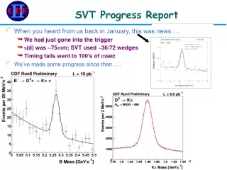
SVT
SVT. Michael Merkin SINP MSU. Tracking Specifications Summary. Performance Expectations of the Detector. SVT : Barrel + Forward Barrel Silicon Tracker ( BST ): Stand Alone Tracker φ -coverage ~ 2 π θ -coverage ~ [35 o , ~125 o ] Momentum resolution ~ 50 [MeV/c]


SVT
E N D
Presentation Transcript
SVT Michael Merkin SINP MSU
Performance Expectations of the Detector • SVT : Barrel + Forward • Barrel Silicon Tracker (BST): Stand Alone Tracker • φ-coverage ~ 2π • θ-coverage ~ [35o, ~125o] • Momentum resolution ~ 50 [MeV/c] • φ-resolution ~ 5 mrad • θ-resolution ~ 20 mrad • Tracking Efficiency >90%
Performance Expectations of the Detector • Forward Silicon Tracker (FST): Works with Drift Chambers • φ-coverage ~ 2π • θ-coverage ~ [5o, ~35o] • Tracking Efficiency >90% • Improve Vertex Resolution • Improve φ-resolution
Design Optimization Four Barrel Regions : 8, 12, 18, 24 modules Three Forward Regions : 15, 15, 15 modules • maximizes momentum resolution • Radii of region 1 and region 4 • minimizes multiple scattering • no overlap of modules • all electronics outside active area • strip layout reduces number of masks needed • strip layout with variable angles reduces dead areas • use of previously designed readout chips (FSSR2)
Background Studies Full Luminosity: FST Rates Summary EM Hadronic Total EM Hadronic Total 1a 1080 3.78 1083 1b 954 3.55 958 2a 895 3.40 899 2b 872 3.47 876 3a 851 3.33 854 3b 894 3.42 897 1a 31.3 2.45 33.7 1b 29.2 2.23 31.5 2a 31.1 2.15 33.3 2b 26.3 2.22 28.6 3a 24.6 2.16 26.8 3b 24.2 2.23 26.4 No Energy Cut E Dep > 20 KeV All rates in MHz
Background Studies Full Luminosity: Radial FST Rates 19.35 MHz 23.87 MHz 28.56 MHz 33.70 MHz y = 19.029 mm Layer 1a
Background Studies Full Luminosity: Radial FST Rates Rate (MHz) mm Transverse distance from beamline
Background Dose, Fluence Studies BST Layer GeV/s GeV/(s cm2) mrads/s mrads/(s cm2) rad/year rad/(year cm2) 1a 7147.8 19.05 4.39 0.011708 138480 369.24 1b 3889.4 10.37 2.38 0.006371 75352 200.92 2a 4578.2 4.06 0.93 0.000833 29566 26.27 2b 3551.7 3.15 0.72 0.000646 22936 20.38 3a 3828.5 1.51 0.34 0.000137 10988 4.34 3b 3295.7 1.30 0.29 0.000118 9459 3.73 4a 3145.5 0.93 0.21 6.360e-05 6771 2.00 4b 2743.3 0.81 0.18 5.547e-05 5905 1.74 1 year = 31,536,000 s
Background Dose, Fluence Studies BST – No Field Layer TeV/s TeV/(s cm2) mrads/s mrads/(s cm2) krad/year krad/(year cm2) 1a 9375.3 24.998 5759.6 15.357 181630 484.31 1b 3013.5 8.035 1851.3 4.936 58381 155.67 2a 2793.4 2.482 572.0 0.508 18039 16.03 2b 1336.4 1.187 273.6 0.243 8630 7.66 3a 1566.2 0.618 142.5 0.056 4495 1.77 3b 875.9 0.346 79.7 0.031 2514 0.99 4a 1021.0 0.302 69.6 0.020 2197 0.65 4b 593.9 0.179 40.5 0.012 278 0.37 1 year = 31,536,000 s
Background Dose, Fluence Studies FST Layer GeV/s GeV/(s cm2) mrads/s mrads/(s cm2) rad/year rad/(year cm2) 1a 3933 3.56 0.85 0.77 27042 24.5 1b 3370 3.05 0.73 0.66 23166 21.0 2a 3288 2.98 0.71 0.65 22609 20.5 2b 3102 2.81 0.67 0.61 21325 19.3 3a 3123 2.83 0.68 0.61 21463 19.6 3b 3094 2.81 0.68 0.61 21269 19.3 1 year = 31,536,000 s
Background Dose, Fluence Studies FST – No Field Layer TeV/s GeV/(s cm2) mrads/s mrads/(s cm2) kilorad/year rad/(year cm2) 1a 52.92 48.00 11.53 10.46 363.8 329.9 1b 43.45 39.41 9.47 8.59 298.7 270.9 2a 39.82 36.12 8.68 7.87 273.7 248.3 2b 35.18 31.91 7.66 6.95 241.8 219.3 3a 32.88 29.83 7.16 6.50 226.0 205.0 3b 28.06 25.45 6.11 5.54 192.9 175.0 1 year = 31,536,000 s
Summary of Sensor Specifications • Single – Sided Construction • Lower cost – higher production yields with less defects • High resistivity (~5kΩ/cm) n-type bulk • Sensor can be fully depleted at relatively low voltage • <100> Surface Orientation • Reduces sensor surface damage due to radiation • Al strips AC coupled to p+ strip implant strips • Protect readout ASIC from DC strip currents • Surface Passivation • To protect the semiconductor surface from electrical and chemical contaminants
Summary of Sensor Specifications • Overhang of AL strips (6 µm) over p+ implants • Improves HV stability of the sensor • Bias Voltage to strips via Polysilicon Resistors • Decouples individual biased AL strips, best radiation performance • Guard Ring • Shapes the electric field at the border of the active area • Outer n++ Protecting Ring • Defines the volume, prevents high field at the sensor’s edge • Low Leakage Current • Reduces noise
BST Sensor Cross Section Hartmann, Frank. Evolution of Silicon Sensor Technology in Particle Physics. Springer Berlin / Heidelberg, 2009.
Sensor Specifications Mechanical Layout Summary Outer Size 42.000 x 111.625 mm Active Area 40.032 x 109.955 mm Dicing Tolerance ± 20µm # of readout strips 256 # of intermediate strips 256 Implant strip pitch 78 µm Readout strip pitch 156 µm Implant strip width 20 µm Aluminum strip width 26 µm Implant width / pitch ratio .256 Angle of strips 0°(strip 1) to 3°(strip 256)
Sensor Specifications Summary of Electrical Properties Full depletion voltage 40<V<100 (25°C@<45%RH) Interstrip capacitance <1.2 pf/cm Leakage current (@ depletion V) <1nA/cm2 Strip to back side capacitance <0.2 pF/cm Interstrip isolation (@150V) >1 GΩ Resistance of Al strips < 20 ohm/cm Coupling capacitance >10 pf/cm Total (strip) capacitance (Ctot = Cint + Cback at 1 MHz) ≤1.3 pf/cm Value of poly-silicon bias resistor 1.5 MΩ Single strip DC current < 3 nA
Sensor Testing Tests by vendor for each sensor: • Sensor Leakage Current • Interstrip, backplane, and total capacitance • Depletion voltage • Interstrip resistance, Poly bias resistors, Al Strip resistance Information to be supplied by the vendor for each sensor: • ID # engraved in the area provided on the sensor • For each wafer, list the sensor ID numbers • Test results for each sensor • Traceability data of processing (batch relative yield, start and end date, and wafer numbers
FSSR2 - Specifications High density – 128 channels / chip Low Power – 3 mW / channel Data driven architecture – no trigger (synchronized with DAq with timestamp clock) Zero suppressed data readout Fast output – 840 Mbit/sec readout capability (1-6 programmable serial outputs) IP License from INFN to procure additional chips
FSSR2 - Validation • Current Test Plan consists of 95 tests exercising all aspects of the ASIC to verify specifications • Test Board created to inject external charge and connect chip to sensor • Document results to aid in collaboration with other facilities • Tests with 1st article SVT modules scheduled for 2010 • CLAS-Notes • 2008-021, 2008-022, 2008-024, 2008-028, 2009-008, 2009-015, 2009-021
ASIC Survey • Options: SVX4, FSSR2
FSSR2 tests Signal= 20000e- Worst case S/N=>10
Signal rate distributions for the laser and injected signal Signal= 20000e-