Download
1 / 27
270 likes | 392 Views
The MROD-1 hardware overview encompasses MRODin and MRODout interfaces, detailing the FPGA architecture, including memory management, VME64x interface, and SHARC links. It highlights key features such as buffer memory, fault tolerance mechanisms, and dataflow control. The document provides insights into interrupt sources, data formatting, and error handling processes. Real-life examples illustrate Tetris register operations and data handling procedures. The MRODig architecture ensures efficient and reliable data processing for high-performance applications.

E N D
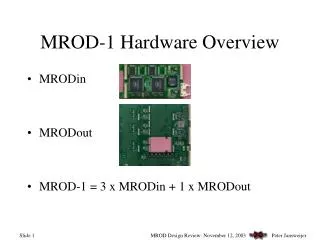
MROD-1 Hardware Overview • MRODin • MRODout • MROD-1 = 3 x MRODin + 1 x MRODout
MROD-1 Hardware Overview MRODout FPGA Memory VME64x 1 SHARC 4 MRODin 3 C 2 FPGA SHARC A 1 0 Memory 2 FPGA Memory 3 4 5 6x S-Link or GOLA LVDS Out 1 SHARC 4 SHARC Links MRODin 3 D 2 FPGA LVDS In Memory SHARC B 1 4 5 2 FPGA Memory FPGA 3 0 1 SHARC 4 MRODin 3 E 2 FPGA TTC interface Memory
MRODin • Buffer memory, Separate partition per TDC, Dataflow into the buffer memory • Tetris register, I2O-FIFO, Fault tolerance, Error signaling and handling , Resynchronization • Dataflow out of buffer memory, DMA, Zero suppression, Length FIFO • Data format, TDC-ID, Parity errors • Interrupt sources • FPGA registers
MRODin Overview S-Link or GOLA FIFO Input 1 MB ZBT Buffer Memory Output Tetris Register I2O FIFO Control Data FIFO Length FIFO 4 Sharc links 40 (80) MB/S Each Control/Status Error signaling FPGA Channel A SHARC S-Link or GOLA Channel B Memory FPGA Channel B
Buffer Memory PartitionsDataflow into buffer memory Separator = Start new TDM Cycle S Note: TDC headers are omitted for simplicity! No Data = Time slot filler N TDC data word T TDC trailer Time Division Multiplexed 0 1 2 3 4 5 0 1 2 3 4 5 0 1 2 3 4 5 0 1 2 3 4 5 S T N T T S T T T T S T T T T N S T N T T T T T T T T T T T T TDC 4 TDC 5 TDC 0 TDC 1 TDC 2 TDC 3 In real life: 18 Buffer Memory Partitions (8 K words each)
Tetris RegisterNormal operation Example Tetris Register = 6 x 4 In real life, Tetris Register = 18 x 16 All trailers of Event-ID n arrived n+3 n+4 Expected Event-ID n n+1 TDC 1 TDC 2 TDC 5 TDC 0 TDC 3 TDC 4 I2O-FIFO Event-ID n
Tetris RegisterTDC trailer missed All trailers of Event-ID n+1 arrived n+3 n+5 Expected Event-ID n n+2 I2O-FIFO TDC 1 TDC 2 TDC 5 TDC 0 TDC 3 TDC 4 Event-ID n+1 Event-ID n
Tetris RegisterNotorious absence of TDC(panic mode) Arrival of a trailer for Event-ID n+3 n+3 n+4 Expected Event-ID n n+1 I2O-FIFO TDC 1 TDC 2 TDC 5 TDC 0 TDC 3 TDC 4 Event-ID n
Tetris RegisterEarly / Late Early TDC1 trailer n+4 n+4 Expected Event-ID n+1 n+1 Late TDC 1 trailer TDC 1 TDC 2 TDC 5 TDC 0 TDC 3 TDC 4 • Notes: • Expected Event-ID can be set by the SHARC during MRODin initialization • Expected Event-ID is hardware updated • Resynchronization for an MRODin channel should be possible.
Buffer Memory PartitionsDataflow out of buffer memory TDC 4 TDC 5 TDC 0 TDC 1 TDC 2 TDC 3 • When a TDC is not present then don’t read the partition! You’ll never encounter a Trailer! • This information is signaled in the data stream (TLP word) T T T T T Read from I2O-FIFO: T T T T T T T Event-ID n Trailer and Word Count (TWC) Word Count and Event-ID TDC Link Present (TLP) word 0 1 2 3 4 5 T T T T T T To Output Data FIFO (128) To Length FIFO (128)
Dataflow out of buffer memoryContinued • Output Data FIFO is read with continuous DMA by the SHARC • Length FIFO provides event summary • While reading TDC data from buffer memory, data can be zero suppressed (i.e. TDC header immediately followed by TDC trailer)
Data Format:TDC-ID in TDC Header word 31-28 27-24 23-0 TDC word received by CSM TDC-ID (4-bit) Upper Nibble = TDC data type 0x1010 TDC Header 0x1011 End Of TDC Group (used by AMT-1; Not used by AMT-2/3 chip) When the MRODin encounters a TDC Header, it reformats the TDC-ID bits: 31-29 28-24 23-0 5-bit TDC-ID based on TDM time slot TDC Header With 5-bits, 18 TDCs can be coded See: T. Wijnen, “The MROD data format”, (ATL-COM-MUON-2003-011) http://www.hef.kun.nl/atlas/
Data Format: Parity errors 31-28 27-24 23-0 TDC word received by CSM TDC-ID (4-bit) Upper Nibble = TDC data type 31-28 27 26 25-24 23-0 TDC word received by MROD 2 bits, residue from TDC-ID CSM -> MROD Parity bit TDC -> CSM Parity Error Upper Nibble = TDC data type When the MRODin encounters a TDC Parity Error or an Input Link Parity Error, it replaces the upper nibble with an Error replacement code (programmable) 31-28 27-24 23-0 Upper Nibble Error Replacement Code
MRODin Interrupts • IRQ0 XI2O_FIFO Full (128 entries) XS Buffer Memory Partition Full (8 K words) S Read Out Maximum TDC Parity error (+ Overrun) • IRQ1 Input Link Parity error (+ Overrun) Input Link Down • IRQ2 TDC Early, Late (+ Overrun) Notes: X: Fatal S: Shutdown Read-out for particular TDC All interrupt sources are individually mask-able
MRODin FPGA Registers • msb’s MRODin Header Pattern (TLP) • msb’s MRODin Trailer Pattern (TWC) • Event Length FIFO • Interrupt Control IRQ0 • I2O_FIFO Full • Buffer Memory Partition Full • Read-out Maximum • TDC Parity Error (Overrun) • TDC Parity Error Individual Interrupt Mask • Input Link Interrupt IRQ1 • Input Link Parity error (Overrun) • Input Link Down • Early and Late Event-ID IRQ2 • TDC number, Event-ID (Overrun) • Test & Input Link Control Status Register • Test Link Data Register • Test Link Control Register • Maximum Event Size • Expected Event-ID • TDC Mask Register • Partition Read-out Enable • Separator Flags Register • Separator • Pattern • Control Bit Pattern • Mask • Control Bit Mask • TDC Header • Pattern • Control Bit Pattern • Mask • Control Bit Mask • TDC Trailer • Pattern • Control Bit Pattern • Mask • Control Bit Mask • No Data • Pattern • Control Bit Pattern • Mask • Control Bit Mask • Error-Code Replace Patterns
Summary MRODin • Event building of TDC data • Tetris register creates a fault tolerant design • FPGAs supply SHARCs with appropriate (error) information • Testable by SHARC via access to registers and memory
MRODout MRODout VME64x 1 SHARC A 0 • VME64x Interface • TTC Interface via TIM • FIFO and Flow control via ROL • Interrupt sources • FPGA registers 2 3 4 5 LVDS Out SHARC Links LVDS In SHARC B 1 4 5 2 FPGA 3 0 TTC interface
VME64x Slave Interface VME64x Guideline; Chris Parkman, “ATLAS Read Out Driver VMEbus Implementation”: http://atlas.web.cern.ch/Atlas/GROUPS/FRONTEND/documents/ROD_VME83.pdf • CR/CSR (AM 0x2F) • A24/D32 Single Cycle Mandatory • A24/D32/D16/D08(EO)/D08(O) Single Cycle, RMW Optional • SHARCs • A32/D32 Single Cycle, RMW, BLT Preferred • CR full VME64x range, currently filled with the VME64 subset • CSR BAR/BitSet/BitClr registers • SHARC may generate a VMEbus Interrupt • Selectable IRQ level [1..7] {I(n) D08(O) where n=1..7} • Programmable 8-bit Status-ID • ROACK Preferred • AM 0x10 (User Defined) used as HARD Reset for the SHARCs
TTC Interface TIM Designed by University College London http://www.hep.ucl.ac.uk/atlas/sct/tim/ • Uses a special P3 backplane with a so called TTC-bus (8 serial signals) • TIM Distributes: • Event-ID / Bunch-ID Put into a FIFO that can be read by the SHARC • Trigger-Type Put into a FIFO that can be read by the SHARC • ECR Connected to SHARC IRQ1 • BCR not used by MROD • L1A not used by MROD • TIM Incorporates Busy Logic to throttle the CTP TTC interface
FIFO and Flow control via ROL • Output S-Link interface 160 MB/s • FPGA contains S-Link Output FIFO (256) to avoid local bus stall due to an XOFF • SHARCs can transfer output data through a chained DMA
MRODout Interrupts • IRQ0 S-Link Return Lines (LRL) Change S-Link LDOWN • IRQ1 Event Counter Reset (ECR) • IRQ2 Event/Bunch-ID FIFO Full Trigger Type FIFO Full All interrupt sources are individually mask-able
MRODout FPGA Registers • VMEbus IRQ • IRQ Level • 8-bit Status-ID Pattern • VMEbus BAR and IRQ • Trigger VMEbus IRQ • IRQ Pending Status • BAR • S-LINK Status and Interrupt Register • Link Return Lines (LRL) • LRL Change Interrupt • Link Down Interrupt • TTC Control/Status and Interrupt Register • Event-ID/Bunch-ID/Trigger Type FIFO Empty/Full status • Event-ID/Bunch-ID/Trigger Type FIFO Full Interrupt • FIFO Flush select (Software or ECR) • Resets and LEDs
Summary MRODout • Event building of data from 3 (/4) MRODin boards • Formatting of the output data for the ROL • Testable by SHARC via access to register
Questions? MRODin MRODout