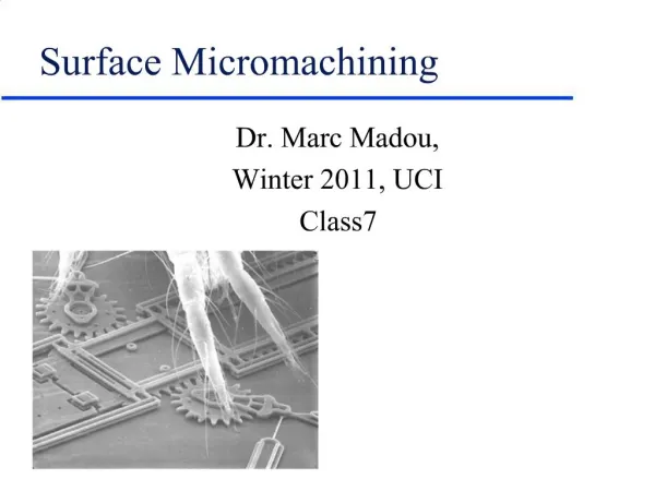
Surface micromachining
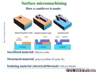
Surface micromachining. How a cantilever is made:. http://www.darpa.mil/mto/mems. Sacrificial material : Silicon oxide Structural material : polycrystalline Si (poly-Si) Isolating material (electrical/thermal): Silicon Nitride. Silicon oxide deposition. SiH 4 + O 2.


Surface micromachining
E N D
Presentation Transcript
Surface micromachining How a cantilever is made: http://www.darpa.mil/mto/mems Sacrificial material: Silicon oxide Structural material: polycrystalline Si (poly-Si) Isolating material (electrical/thermal):Silicon Nitride
Silicon oxide deposition SiH4 + O2 LTO: Low Temperature Oxidation process • For deposition at lower temperatures, use • Low Pressure Chemical Vapor Deposition (LPCVD) • SiH4 + O2 SiO2 + 2H2 : 450 oC • Other advantages: • Can dope Silicon oxide to create PSG (phospho-silicate glass) • SiH4 + 7/2 O2 + 2 PH3 SiO2:P + 5 H2O : 700 oC • PSG: higher etch rate, flows easier (better topography) 425-450 oC 0.2-0.4 Torr
Case study: Poly-silicon growth SiH4 Amorphous film 570 oC Crystalline film 620 oC • by Low Pressure Chemical Vapor Deposition • T: 580-650 oC, P: 0.1-0.4 Torr • Effect of temperature • Amorphous Crystalline: 570 oC • Equi-axed grains: 600 oC • Columnar grains: 625 oC • (110) crystal orientation: 600 – 650 oC • (100) crystal orientation: 650 – 700 oC Kamins,T. 1998 Poly-Si for ICs and diplays, 1998
Poly-silicon growth • Temperature has to be very accurately controlled • as grains grow with temperature, increasing surface • roughness, causing loss of pattern resolution and stresses in • MEMS • Mechanisms of grain growth: • Strain induced growth • - Minimize strain energy due to mechanical deformation, doping … • - Grain growth time • 2. Grain boundary growth • - To reduce surface energy (and grain boundary area) • - Grain growth (time)1/2 • 3. Impurity drag • - Can accelerate/prevent grain boundary movement • - Grain growth (time)1/3
Grains control properties • Mechanical properties • Stress state:Residual compressive stress (500MPa) • - Amorphous/columnar grained structures: Compressive stress • - Equiaxed grained structures: Tensile stress • Thick films have less stress than thinner films • ANNEALING CAN REDUCE STRESSES BY A • FACTOR OF 10-100 • Thermal and electrical properties • Grain boundaries are a barrier for electrons • e.g. thermal conductivity could be 5-10 times lower (0.2 W/cm-K) • Optical properties • Rough surfaces!
Silicon Nitride SiH2Cl2 + NH3 (for electrical and thermal isolation of devices) r: 1016W cm, Ebreakdown: 107 kV/cm • Is also used for encapsulation and packaging • Used as an etch mask, resistant to chemical attack • High mechanical strength (260-330 GPa) for SixNy, provides structural integrity (membranes in pressure sensors) • Deposited by LPCVD or Plasma –enhanced CVD (PECVD) LPCVD: Less defective Silicon Nitride films PECVD: Stress-free Silicon Nitride films x SiH2Cl2 + y NH3 SixNy + HCl + 3 H2 700 - 900 oC 0.2-0.5 Torr
Depositing materialsPVD (Physical vapor deposition) • Sputtering: DC (conducting films: Silicon nitride) RF (Insulating films: Silicon oxide) http://web.kth.se/fakulteter/TFY/cmp/research/sputtering/sputtering.html
Depositing materialsPVD (Physical vapor deposition) • Evaporation (electron-beam/thermal) Commercial electron-beam evaporator (ITL, UCSD)
Electroplating Courtesy: Jack Judy • Issues: • Micro-void formation • Roughness on top surfaces • Uneven deposition speeds • Used extensively for LIGA processing e.g. can be used to form porous Silicon, used for sensors due to the large surface to volume ratio
Depositing materials –contd.- • Spin-on (sol-gel) • e.g. Spin-on-Glass (SOG) used as a sacrificial molding material, processing can be done at low temperatures Dropper Si wafer
Surface micromachining - Technique and issues - Dry etching (DRIE) Other MEMS fabrication techniques - Micro-molding - LIGA Other materials in MEMS - SiC, diamond, piezo-electrics, magnetic materials, shape memory alloys … MEMS foundry processes - How to make a micro-motor
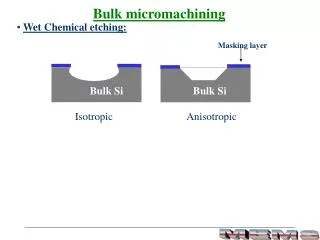
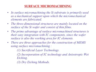
Surface micromachining Carving of layers put down sequentially on the substrate by using selective etching of sacrificial thin films to form free-standing/completely released thin-film microstructures http://www.darpa.mil/mto/mems HF can etch Silicon oxide but does not affect Silicon Release step crucial
Release of MEMS structures • A difficult step, due to surface tension forces: Surface Tension forces are greater than gravitational forces ( L) ( L)3
Cantilever Si substrate Release of MEMS structures • To overcome this problem: • Use of alcohols/ethers, which sublimate, at release step • Surface texturing • Supercritical CO2 drying: avoids the liquid phase 35oC, 1100 psi
A comparison of conventional vs. supercritical drying
Reactive Ion Etching (RIE) DRY plasma based etching http://www.memsguide.com • Deep RIE (DRIE): • Excellent selectivity to mask material (30:1) • Moderate etch rate (1-10 mm/minute) • High aspect ratio (10:1), large etch depths possible
Deep Reactive Ion Etching (DRIE) A side effect of a glow discharge polymeric species created Plasma processes: Deposition of polymeric material from plasma vs. removal of material Usual etching processes result in a V-shaped profile Bosch ProcessAlternate etching (SF6) +Passivation (C4F8) • Bowing: bottom is wider • Lag: uneven formation
Gas phase Silicon etching • Room temperature process • No surface tension forces • No charging effects • Isotropic XeF2 BrF3 Developed at IBM (1962) Developed at Bell labs (1984) 2 XeF2 + Si 2 Xe + SiF4 4 BrF3 + 3 Si 2 Br2 + 3 SiF4 Cost: $150 to etch 1 g of Si $16 for 1 g of Si Etching rate: 1-10 mm/minute
Micro-molding • For thick films (> 100 mm) • HEXSIL/PDMS, compatible with Bio-MEMS C. Keller et al, Solid state sensor & actuator workshop, 1994 - loss of feature definition after repeated replication - Thermal and mechanical stability
LIGA (LIthographie, Galvanoformung, Abformung) • For high aspect ratio structures • Thick resists (> 1 mm) • high –energy x-ray lithography ( > 1 GeV) • Millimeter/sub-mm sized objects which require precision Mass spectrometer with hyperbolic arms Electromagnetic motor
Technology Comparison Bulk vs. Surface micromachining vs. LIGA
Materials in MEMS Mechanical MEMS (for micro-motors etc.) Si, quartz (SiO2), Si3N4, Ti, Ni, permalloy (NiFe), polycrystalline Si … RF-MEMS (for wireless communications): Compound semiconductors: GaAs, InP, GaN Si, SiO2 … Bio-MEMS (micro-electrode arrays, DNA probes) enzymes, antigen/antibody pairs, DNA, polyimides, hydrogels, plastics, porous Si, C, AgCl…
METALS used for wiring (Al, Cu), etch masks (Cr), structural elements (Al, W) - excellent electrical conductors - prone to fatigue SMA : Shape memory alloys(NiTi: Nitinol) Reversible temperature induced transformation from a stiff austenite phase (Y.S.: 550 MPa) to a ductile martensite (Y. S.: 100 MPa) phase. - used for thermal actuation - Can exert stresses of up to 100 MN/m2 - Maximum operating temperature ~ 70 oC - very slow actuation mechanism Polymers: poly-norbornene
Photoresist (PR) Cr/Au Glass substrate Si oxidation Si SiO2 Pattern PR Si etch (KOH) Etch Cr/Au Pattern & deposit NiFe Etch Glass RIE to release cantilever Remove Cr/Au Magnetic materials • prevalent: Ni, NiFe (permalloy), Co alloys • - Not as widely used as electrostatic actuation • - Needs thick films (10-20 mm); using electro-deposition A magnetically actuated cantilever
New applications demand new materials Silicon Carbide (SiC): structural & isolating layer - mechanically robust, E(500 GPa) higher resonance frequency - high temperature material (>200 oC) - difficult to shape (chemically inert) - used in micro-gas turbines Diamond: very hard, for electrical isolation - E: 1035 GPa - excellent thermal conductor, easy heat dissipation - difficult to machine, needs oxygen-plasmas - used in Atomic Force Microscope cantilevers GaAs/InP: opto-electronics - good combination of electrical and mechanical properties - high piezo-electric coefficients - sophisticated manufacture for GaAs and InP substrates (Molecular Beam Epitaxy)
Polymers: structurally compliant • - 50 times lower E compared to Si/Silicon nitride • - Can withstand large strains (100%) • Polyimide: used in force sensor, shear stress • sensor skin • Piezoelectrics: have a mechanical response to an • electric field: ZnO, (Pb,Zr)TiO3 • - Large mechanical transduction, force sensors