Download
1 / 50
730 likes | 1.4k Views
a STIMESI II tutorial 23.02.2011. Wet Bulk Micromachining – . Per Ohlckers, Vestfold University College www.hive.no Per.Ohlckers@hive.no. Daniel Lapadatu, SensoNor Technologies www.multimems.com daniel.lapadatu@sensonor.no. Outline. 1. Background and Motivation 2. The Silicon Crystal

E N D
a STIMESI II tutorial23.02.2011 Wet Bulk Micromachining – Per Ohlckers, Vestfold University College www.hive.noPer.Ohlckers@hive.no Daniel Lapadatu, SensoNor Technologies www.multimems.comdaniel.lapadatu@sensonor.no
Outline 1. Background and Motivation 2. The Silicon Crystal 3. Isotropic Wet Etching 4. Anisotropic Wet Etching 5. Selective Etching 6. Convex Corners
Outline 1. Background and Motivation 2. The Silicon Crystal 3. Isotropic Wet Etching 4. Anisotropic Wet Etching 5. Selective Etching 6. Convex Corners
Manufacturing Processes Serial (e.g. Focused Ion Milling - FIB) vs.batch (e.g. bulk Si micromachining) vs.continuous (e.g. doctor’s blade). Additive (e.g. evaporation) or subtractive (e.g. dry etching). Projection (almost all lithography techniques) vs. truly 3D. Moldvs.final product. FIB There are many different techniques that are being used. However, in general, batch processing is the most powerful technique and used mostly.
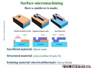
Micromachining Bulk Micromachining is a process that produces structures inside the substrate by selective etching. Surface Micromachining is a process that creates structures on top of the substrate by film deposition and selective etching. Bulk Micromachining Surface Micromachining
Classification of Bulk Silicon Etching Bulk Micromachining is a process that produces structures inside the substrate by selective etching. Wet Etching Dry Etching Crystal orientation dependent Process dependent Isotropic Anisotropic Isotropic Anisotropic AcidicEtchants AlkalineEtchants BrF3XeF2 F-basedplasmas
Etching Features Etch rate: Rate of removal of material/film. Varies with concentration, agitation and temperature of etchant, porosity and density of etched film. Etch selectivity: Relative etch rate of mask, film and substrate. Etch geometry: Etching depth (R); Mask undercut (U); Slope of lateral walls (S); Bow of floor (B); Anisotropy.
Bulk Silicon Etching: Examples Deep cavity by wet, anisotropic etching Release etch by RIE Recess etch by RIE
Wet Silicon Etching: Examples Isotropic etching with HNA (HF : Nitric Acid : Acetic Acid) Anisotropic etching with KOH (110) (100)
Outline 1. Background and Motivation 2. The Silicon Crystal 3. Isotropic Wet Etching 4. Anisotropic Wet Etching 5. Selective Etching 6. Convex Corners
Structure of Single Crystal Silicon Face-centred cubic (fcc) structure (diamond structure) with two atoms associated with each lattice point of the unit cell. One atom is located in position with xyz coordinates (0, 0, 0), the other in position (a/4, a/4, a/4), a being the basic unit cell length. Lattice constant a = 5.43 Å. The arrangement of the silicon atoms in a unit cell, with the numbers indicating the height of the atom above the base of the cube as a fraction of the cell dimension.
Miller Indices Miller indices are a notation system in crystallography for planes and directions in crystal lattices. A lattice plane is determined by three integers h, k and l, the Miller indices, written (hkl). The indices are reduced to the smallest possible integers with the same ratio. Determining the Miller indices for planes by using the intercepts with the axes of the basic cell.
Determining Miller Indices Example: Take the intercepts of the plane along the crystallographic axes, e.g.2, 1 and 3. The reciprocal of the three integers are taken: 1/2, 1/1 and 1/3. Multiply by the smallest common denominator (in this case 6): 3, 6 and 2. The Miller indices of the plane are: (362).
Crystallographic Planes and Directions (abc) denotes a plane. {abc} denotes a family of equivalent planes. [abc] denotes the direction perpendicular on (abc) plane. <abc> denotes a family of equivalent directions. {100}, {110} and {111} are the most important families of crystal planes for the silicon crystal.
Single Crystal Silicon Wafers Primary and secondaryflats indicate the dopanttype and surfaceorientation. Wafer diameter in current fab standards: from 100 to 300 mm. Wafer thickness in current fab standards: from 250 to 600 µm. Surface orientation: (100) for MOS and MEMS; (110) for MEMS; (111) for bipolar. Secondary flat Primary flat
Standard 100 mm Wafers The position of the flat(s) indicates the surface orientation and the type of doping. The primary flat on (100) and (110) wafers is along the [110] direction. Orientation of flats for 100 mm wafers p-(111) n-(111) p-(100) n-(100) Secondary flat Primary flat
Wafers Used in MultiMEMS P-type, 150 mm Si wafer. (100) ± 0.5º Surface. [110] ± 0.5º Primary Flat. Si Wafer
Outline 1. Background and Motivation 2. The Silicon Crystal 3. Isotropic Wet Etching 4. Anisotropic Wet Etching 5. Selective Etching 6. Convex Corners
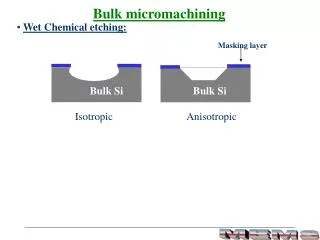
Isotropic Wet Etching of Silicon All crystallographic directions are etched at the same rate. Features: Etchants are usually acids; Etch temperature: 20... 50 °C; Reaction is diffusion-limited; Very high etch rate (e.g. up to 50 µm/min); Significant mask undercutting. Masking is very difficult: Au/Cr or LPCVD Si3N4 is good. SiO2 may also be used for shallow etching. with stirring without stirring Si
Isotropic Etching of Silicon: Etchants Etchant (Diluent) Typical Composition Temp. Etch Rate[µm/min] HF HNO3 CH3COOH + H2O 10 ml 30 ml 80 ml 22 °C 0.7... 3.0 HF HNO3 CH3COOH + H2O 25 ml 50 ml 25 ml 22 °C 40 HF HNO3 CH3COOH + H2O 9 ml 75 ml 30 ml 22 °C 7.0 Mechanism HNO3+ H2O + HNO2→ 2HNO2 + 2OH–+ 2h+ Si4+ + 4OH–→ SiO2 + H2 SiO2+ 6HF → H2 SiF6 hole injection: oxidation: oxide removal:
Silicon Etching with HNA HNA: mixture of 49,23% HF, 69,51% HNO3 and acetic acid (CH3COOH) or water (H2O) as diluent. HNO3 oxidizes the silicon, HF removes the oxide: High HNO3:HF ratio,- Etch limited by oxide removal. Low HNO3:HF ratio- Etch limited by oxide formation. Dilute with water or acetic acid: CH3COOH is preferred because it prevents HNO3 dissociation. (µm/h) Iso-Etch Curve (from Robbinset al.)
Isotropic Etching of Glass Single- or double-side etching of glass wafers is achieved either by using HF-water solution or HNA. Typical etch rate for borosilicate glass in HNA: 1.9 µm/min. Applications: Etching cavities and through-holes; Etching gas/fluid channels. Through-hole Mask Cavity Undercut
Outline 1. Background and Motivation 2. The Silicon Crystal 3. Isotropic Wet Etching 4. Anisotropic Wet Etching 5. Selective Etching 6. Convex Corners
Anisotropic Wet Etching of Silicon Crystallographic directions are etched at different rates. Features: Etchants are usually alkaline; Etch temperature: 85... 115 °C; Reaction is rate-limited; Low etch rate (ca. 1 µm/min); Small mask undercutting. Masking is very difficult: LPCVD Si3N4 is good; SiO2 may also be used with some etchants. Si
Etching Setup Laboratory setup for wet chemical etching of silicon. The principles for industrial manufacturing equipment are the same.
Anisotropic Etching of Silicon: Etchants Etchant (Diluent) Typical Composition Temp. Etch Rate [µm/min] Etch Ratio (100)/(111) Masking Film Etylenediamine Pyrocathecol Water 750 ml 120 gr 100 ml 115 °C 0.75 35:1 SiO2 Si3N4 metals Etylenediamine Pyrocathecol Water 750 ml 120 gr 240 ml 115 °C 1.25 35:1 SiO2 Si3N4 metals KOH Water + Isopropyl 44 gr 100 ml 85 °C 1.4 400:1 SiO2 Si3N4 TMAH Water + Isopropyl 220 gr 780 ml 90 °C 1.0 100:1 SiO2 Si3N4
Chemistry of Anisotropic Etching Etching phases: Transport of reactants to the silicon surface; Surface reaction; Transport of reaction products away from the surface. Key etch ingredients: Oxidisers; Oxide etchants; Diluents and transport media. Mechanism Si + 2OH–→ Si(OH)22+ + 4e– 4H2O + 4e–→ 4OH– + 2H2 (gas) Si(OH)22+ + 4OH–→ SiO2(OH)22– + 2H2O Overall: Si + 2OH– + 2H2O → → SiO2(OH)22– + 2H2 (gas)
Anisotropic Etching of (100)-Si Cavity defined by: {111} walls slow-etching planes; {100} floor fast-etching plane. Final shape of cavity depends on: Mask geometry; Etching time. Shape of cavity: Truncated pyramid; V-groove; Pyramid.
Cavity Geometry for (100)-Si Wb = W0 – 2·l·cot(54.7°) Anisotropically etched cavity in (100) silicon with a square masking film opening oriented parallel to the <110> directions.
Mask Undercutting (a) is a pyramidal pit bounded by the {111} planes. (b) is a type of pit expected from slowundercutting of convex corners. (c) is a type of pit expected from fastundercutting of convex corners. In (d), further etching of (c) produces a cantilever beam suspended over the pit. (e) illustratates the general rule for undercutting assuming a sufficiently long etching time.
Anisotropic Etching of (110)-Si Cavity defined by: {111} walls slow-etching planes; {110} floor fastest-etching plane; {100} bottom side walls fast-etching planes; Final shape of cavity depends on: Mask geometry; Etching time. Cavity shape: Rhombic prisms; Hexahedric prisms.
Outline 1. Background and Motivation 2. The Silicon Crystal 3. Isotropic Wet Etching 4. Anisotropic Wet Etching 5. Selective Etching 6. Convex Corners
Methods for Selective Etching Time etching methods: Calculate the needed etching time on the basis of the etching rate. Easy, but inaccurate method, as etching rate varies with the chemical condition of the etchant and geometrical factors limiting the agitation of the etch. Typical accuracy: ± 20 µm. Inspect the depth of the etched cavity in appropriate time intervals until desired depth is reached. Time consuming, but improved accuracy. Uneven etching depth from cavity to cavity due to chemical and geometrical factors is still a problem. Typical accuracy: ± 10 µm. Chemical selective techniques: The etching stops when a chemically resistive layer is reached. Typical accuracy: ± 3 µm. Electrochemical selective techniques: The etching stops on reverse biased pn junctions. Typical accuracy: ± 1 µm.
Time-Stopped Etching Example of etching stopped at an arbitrary depth, exhibiting a flat floor.
Etching Stopped by {111} Walls Example of etching stopped by the intersecting {111} walls, exhibiting a pyramidal groove.
Boron Etch-Stop Technique Chemical selective etching: Etch rate depends on boron concentration. Etching stops if boron concentration exceeds 5·1018 cm–3. Boron stop layer is manufactured: By diffusion deposition, implantation or both; On the opposite surface of the wafer with respect to the etch cavity. Boron-dependent etch rate of silicon (from Seidelet al.)
Boron Etch-Stop Mechanism Interstitial bonds require more energy to be broken. The electrons supplied by the etchant recombine with the holes in the bulk, rather than participating in the chemical reaction. Interstitial boron atom Substitutional boron atom Silicon atom
Boron Etch-Stop Shortcomings Electronics cannot be integrated in the boron stop layer. Solution: depositing an epitaxial layer atop the stop layer, with appropriate doping as substrate material for integrated devices. Controlling the autodoping of the epi-layer is challenging. n-type epitaxial layer p+ type boron stop layer n-type substrate
Electrochemical Etch-Stop (ECES) Electrochemical selective etching: Etch rate depends on the applied potential. Etching stops if the applied potential exceeds a threshold value, called passivation potential. Low-doped material, both p- and n-type, can be passivated: To be used as substrate for integrated components such as piezoresistors. High accuracy, typically ± 1 µm: Achieved by using well-controlled implantation and diffusion techniques. KOH and TMAH can be used: Both avoid the health dangers of EDP.
Wafer Holder for ECES A practical way to make a wafer holder to be used for electro-chemical selective etching. The principles for industrial manufacturing equipment are the same.
Electrochemical Etch-Stop Mechanism Etch-stop achieved by reverse biasing the pn junctions. More in the Bulk Silicon Etching tutorial...
ECES for MultiMEMS Electrochemical etch-stop allows 3 different thicknesses: Full-wafer thickness (400 µm) For heavy seismic masses; Epi-layer thickness (3 µm) For thin membrane, springs; N-well thickness (23 µm) For thick membranes, masses, bosses…
Etch-Stop on Multi-Level Junctions Very Thin Membrane Thick Membrane (Mass/Well) Thin Membrane
Outline 1. Background and Motivation 2. The Silicon Crystal 3. Isotropic Wet Etching 4. Anisotropic Wet Etching 5. Selective Etching 6. Convex Corners
Undercutting of Convex Corners High etch-rate of high-index planes: Severe undercutting of convex corners; Truncated pyramids or V-grooves as final cavities. Mask will be undercut until {111} planes are exposed. Mask {111}
Compensation for Convex Corners Etching without corner compensation structure Etching with corner compensation structure Corner Compensation in Silicon (from Guptaet al.) Corner compensation of mask is difficult to establish as a repeatable process; highly dependant on etching parameters.
Corner Compensation Structures Compensation Structure Desired Result A simple approach to convex corner compensation (from Wei Fanet al.)
Designing with Undercut Corners Fabrication of MEMS - MEMS Technology Seminar(from Burhanuddin Yeop Majlis)
Thank you for your attention !