Download
1 / 62
670 likes | 1.03k Views
SOI High Aspect Ratio Micromachining. www.tronics.eu. Dr. Joël COLLET Senior Engineer. 1. TRONICS Microsystems introduction. Dr. Joël COLLET Senior Engineer. Facts & Figures. Activity: Developer and contract manufacturer of custom MEMS components for demanding applications

E N D
SOI High Aspect Ratio Micromachining www.tronics.eu Dr. Joël COLLET Senior Engineer
1. TRONICS Microsystems introduction Dr. Joël COLLET Senior Engineer
Facts & Figures • Activity: Developer and contract manufacturer of custom MEMS components for demanding applications • Creation: Spun-off from CEA-LETI in 1997 • Locations: Crolles, France, manufacturing facility • Facilities: 1350m² with 750m² for production, packaging and test Incl. 400m² clean rooms, 6’’ wafers • Funding: 15 M€ in 4 rounds • Revenues: 6.2M€ in 2005, amongst the 200 fastest growing EMEA company • Staff: 46 (26 prod., 12 R&D, 8 sales & admin.) • Expertise: Custom high performance SOI-MEMS manufacturing
Business model Developer and Contract Manufacturer of high value-add MEMS-based custom components for demanding applications • Customization/industrialization of existing solutions/platforms • from the customer • from third parties • from our own • Contract manufacturingof custom components Your Strategic Manufacturer of Custom MEMS components
End-to-end development and manufacturing service Process developmentand qualification ASIC development support and/or management Design for manufacturing, modelling and simulation Packaging development and optimization Testing, characterizationreliability and quality control Industrialization and Supply chain management Expert services for the industrialization of your custom MEMS product
Through partnerships 10 K 1 M 100 K 10 M 100 M Market FocusCustom MEMS components for demanding applications Aerospace/Défense 100 / Instrumentation Telecom networks MEMS Value-added 10 Life Sciences BioMedical Building automation Automotive 1 IT, mobile and consumer products Volume (pieces/year)
Pioneer of Custom SOI MEMS Manufacturing Unique Generic Industrial SOI Technology Platform DRIE on Thick SOI Sacrificial/Cavity release Wafer Level Packaging Miniature accelerationtransducer Geophone, extreme resolution accelerometer 16 bits, High performanceAcceleration sensors Resonating Gyrometers For High Performance Custom MEMS Components
2. From bulk µmachining to SOI-HARM Dr. Joël COLLET Senior Engineer
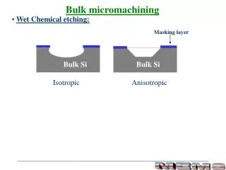
Silicon Bulk Micromachining: The 80s Typical piezo-resistive pressure sensor process B+ Ion implantation Thermal annealing & hole opening Metal deposition and patterning Implanted strain gauge Si/Glass Anodic Bonding Back side KOH etching vacuum • Single crystal Si • Batch processing techniques, simple technologies = > Low cost • Design limitation => large components, high cost • Big masses, beams and membranes = > High Performance possible
Silicon Surface Micromachining: The 90s Typical surface micromachining process Sandia Lab Deposition of SiO2Deposition of Poly-SiThickness = Few µ-meters Photolitho of pattern Etching of Poly-Si Selective etching of SiO2 as “Sacrificial layer” • High integration and miniaturization = > Low cost • Limitation on active layer thickness (<15µm) = > Performance limitation • Perfect candidate for low cost / low perf / high volume applications • Resistance to long term mechanical fatigue ?
SOI surface micromachining and HARM: The 21st century • High integration and miniaturization => Low cost • Very thick layer (10µm < x < 150µm) => High performance • Single crystal silicon: High reliability • Simplified process: higher yield • SOI wafers: expensive material • Perfect candidate for high performance/medium volume applications
Low vacuum sealed cavity Opening for light, fluids, gas or vacuum Gold contacts Si = 300µm Si = 60µm BOX=2µm Si = 450µm Hermetic Sealing HF release DRIE > 1:20 Min. gap: 3µm Min. Feat.: 4µm An industrial environment for training and innovation SOI-HARM with hermetic package
SOI Wafer Process flow Deposit metal Pattern seal and contact area BSOI wafer, P type doped, 10-20 mOhm.cm, 60 µm/2µm/450 µm HARM etching Sacrificial etching
Cap Wafer Process flow Thermal oxidation Si wafer, P type doped, 10-20 mOhm.cm, 300 µm Oxide etching (cavity pattern) Etch oxide back Deposit and pattern cap contact Deposit metal pattern seal area
Assembly Process flow Pattern the VIA Etch thermal oxide Wafer preparation for sealing Apply pressure and temperature Final device with hermetic and non hermetic contact
SOI HARM • Deep DRIE: High Aspect Ratio Micromachining • Principles • Use the faculty of some gases mixtures in plasma to perform etching (mainly isotropic) or deposition • By alternating deposition (C4F8 gases) and etching (SF6 gases) phases (so-called Bosch process) it is possible to perform anisotropic vertical etching with high aspect ratio feature (over 1:20)
SOI HARM Deep Etcher description Principle description
SOI HARM SEM view of a Silicon patterned with HARM
SOI HARM Typical DRIE profile in Bulk Silicon With Depth Depending on Trench Width Typical DRIE profile in SOI With Special process in order to avoid over etching of pattern’s feet
SOI HARM • ETCHING DEFINITION • Typical DRIE Trench Profile • Typical DRIE Pattern Profile With over-etching and scalloping • Form Factor : 20:1
Release by Sacrificial Etching • Sacrificial etching • Principles • Use the faculty of concentrated HF (10 to 50%) to etch oxide over a very long distance in very narrow trenches • By drying the structure once released with special process using solvents (avoid sticking due to capillarity)
Release by Sacrificial Etching Principle description
Release by Sacrificial Etching Sticking Effect One of the main issues for MEMS yield in releasing process. Capillarity forces pull the structures to the substrate. IR view of a released beam and a sticked beam
Release by Sacrificial Etching • Wet process. • Specific rinsing and drying. • Sublimation process (cyclohexane, CO2) • lowering the surface tensions • lowering of capillarity effects • Dry process • Etching with HF vapours • End of the releasing with resist • no capillarity effects • Design optimisation • Ratio between surface and gapAnti sticking bumps • increasing the stiffness
Metallic bonding • Metallic bonding • Principles • Use the faculty of some metals to form « low temperature » alloy (Au +Si, Au +Sn) or their softness (Au, Cu) to be thermocompressible • By applying pressure and temperature in a vacuum chamber during a certain amount of time, sufficient to ensure the bonding of the two wafers.
Metallic bonding • Bonding equipment
Metallic bonding • Bonding description, schematic Heat, pressure, time
Metallic bonding SEM and optical view of a metallic seal
5. SOI-HARM – Design Kit Dr. Joël COLLET Senior Engineer
Complete Design Rules Manual DRM available on request
Standard cells available to ease the design Base cell for the external layout Base cell hermetic sealing view Pads cells (hermetic and open)
Supported by a software kit on CoventorWare Use process emulation file and Material properties database Create 2D and 3D designs following design rules Schematic from parametric cells Device behaviour simulation Extract GDSII/CAT for submission Design Kit available on request
CoventorWare Design Kit for Tronics HARM CoventorWare modules are configured for Tronic’s SOI-HARM process in order to easily design with confidence into an established process
CoventorWare Design Kit for Tronic’s SOI-HARM Process • Deliverables: • Materials Property database (*.mpd) of Tronic’s characterized materials • Process emulation file (*.proc) for Tronic’s SOI-HARM process • Layout template file (*.cat, *.gds) • Library of parametric and non-parametric elements supporting schematic and physical design • Validated design handbook including process description and design rules • Available at Tronic’s at no charge • Enabled by DESIGNER TM • Supports complete CoventorWare TM design flow
Design Kit Enables 2D Layout to 3D Solid Model Process, material data 2D Layout Input from schematic Import GDSII, CIF, or DXF files Use process info as template • Extract layout from schematic automatically or draw layout manually • Perform Design Rule Checks • Combine 2D Layout with process description to build a 3D Solid Model and perform FEA • Output masks to be used for fabrication 3D Model GDSII output for mask generation
Design Kit Supports Schematic Driven Design • Tronic’s materials and Process data are shared between schematic and physical design part • Create device schematic from library of MEMS-specific “parametric elements” • Simulate device behavior within sub-system rapidly and accurately • Perform Monte-Carlo and Sensitivity analyses to optimize design Schematic of accelerometer, composed of parametric building blocks representing beams, electrostatic combs and mass – based on Tronic’s process
CoventorWare Design Kit for the SOI-HARM • Key benefits: • Easy and low risk entry into MEMS design and prototype development • Validated in fab runs • Offers inn combination with MPW low cost prototyping • Compatible with CoventorWare standard modules - stable and most widely installed MEMS design tool • Design MEMS with confidence into Tronic’s established and characterized fabrication process • Accelerate Time-To-Market
6. SOI-HARM – Masks Levels Masks Levels Dr. Joël COLLET Senior Engineer
SOI Wafer Reminder: Dark Field means that the data you draw are rendered clear (glass) on the mask Clear Field means that the data you draw are rendered dark (chromium) on the mask
7. SOI-HARM – Design Rules Dr. Joël COLLET Senior Engineer
Nomenclature Design rules defines the minimum feature sizes and spaces for all the levels you are allowed to work on and minimum overlap and spacing between relevant levels - Minimum line widths and spaces are mandatory rules. They are given to ensure that all layouts will remain compatible with TRONIC’S Microsystems lithographic process tolerance. Minimum width
Nomenclature - Minimum spacing between levels guarantees that features of two different levels can be delineated by photolithography and etch. Minimum space Minimum Notch (the minimum spacing between two patterns of a same boundary )
Nomenclature - Minimum overlap requirements are related to the precision of the alignment between different levels and reduce the effect of large topographies. Minimum enclosure (When a boundary B1 in layer L1 surround a boundary B2 in layer L2, a minimum distance between the edge of the boundary B1 and the edge of the boundary B2 can be defined ) Minimum cut-inside (This dimension defines the minimum amount that a layer 1 feature can overlap a layer 2 feature) Minimum cut-outside (This dimension defines the minimum amount that a layer 1 feature can extend beyond a layer 2 feature.)