Download
1 / 18
220 likes | 951 Views
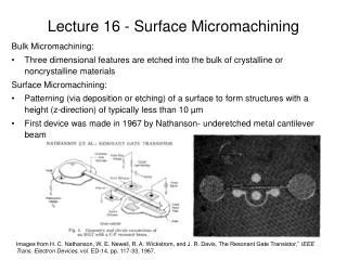
Surface Micromachining. Dr. Marc Madou, Fall 2012, UCI Class 10. L m. Photoresist. Lm + 2t SiO2. Surface Micromachining. n +. Basic Process Sequence (poly-Si). Blanket n + diffusion of Si substrate (ground plane)

E N D
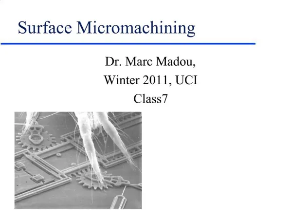
Surface Micromachining Dr. Marc Madou, Fall 2012, UCI Class 10
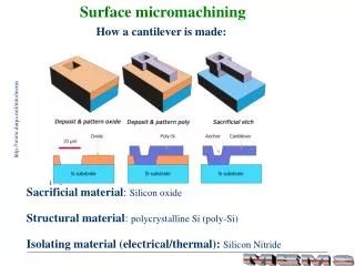
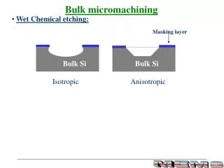
Lm Photoresist Lm + 2tSiO2 Surface Micromachining n+ Basic Process Sequence (poly-Si) • Blanket n+ diffusion of Si substrate (ground plane) • Passivation layer (e.g. SiO2 , Si3N4 , LPCVD Si3N4 on top of SiO2) • Opening up the passivation layer for contacts (observe color change or hydrophobic/hydrophilic behavior): • wet (BHF) • dry (SF6) • Strip resist in piranha (adds some oxide in the window) • Short BHF etch to remove thin oxide n n+ n tSiO2 Si3N4
Deposition of a base, spacer or sacrificial layer-phosphosilicate glass (PSG)-CVD Densification at 950 °C for 30-60 min in wet oxygen Base window etching in BHF for anchors Structural material deposition e.g. poly-Si (doped or undoped) from (CVD at about 600°C , 73 Pa and 125 sccm (standard centimeter cube per minute); at about 100Å/min) e.g. Anneal of the poly-Si at 1050°C for 1 hour to reduce stress in the structure Surface Micromachining PSG nitride Basic Process Sequence (poly-Si). Structural layer
Basic Process Sequence (poly-Si) Surface Micromachining • Doping of poly-Si: in-situ, PSG sandwich and ion implantation • Patterning of structural material e.g. RIE in , say, CF4-O2 • Release step, selective etching of spacer layer e.g. in diluted HF nitride Ri Rm RS
Si Generic principle of surface micromachining Surface Micromachining Al Sacrificial layer definition Etch access Polyimide diaphragm deposition Si Releasing diaphragm: phosphoric/acetic acid/nitric acid (PAN) Si
LPCVD of poly-Si Surface Micromachining • Hot wall, horizontal reactor • Reaction rate controlled--at lower pressures and well controlled temperatures (100 to 200 wafers) • Poly-Si deposits everywhere requiring periodic cleaning (e.g. every 20 runs if each run deposits 0.5 µm) • Visit: http://mems.eeap.cwru.edu/shortcourse/partII_2.html and http://www-mtl.mit.edu:800/htdocs/tutorial.html
Stiction Surface Micromachining • Stiction during release: • Surface tension during drying pulls movable members together (See also room temperature bonding of Si to Si and glass to Si) • Solutions: • Stand-off bumps • Sacrificial polymer • Sacrificial poly-Si links to stiffen the structures • HF vapor • Freeze-drying water/methanol mixtures • Super critical cleaning • Stiction after release: • Hydrophobic monolayers • Rough surfaces • Bumps
Control of film stress Surface Micromachining • With L=150 µm and W=t=2 µm, fo=10 to 100 kHz. • Annealing at high temperature (900-1150°C) • Fine-grained tensile vs large grained compressive • Doping elements • Sandwich doping and annealing. • Vary material composition e.g Si rich Si3N4 • In PECVD: change the RF power and frequency • In sputtering: gas pressure and substrate bias
Control of film stress Surface Micromachining Y • Folding flexures makes the resonant frequency independent of the residual stress but warpage becomes an issue • Corrugated structural members (see above) X
Surface Micromachining Sealing processes • Microshells a wafer level packaging strategy • Thin gaps (e.g. 100 nm) are etched out and then sealed: • Reactive sealing by oxidation • LPCVD deposition
IC compatibility Surface Micromachining Comparison of CMOS and Surface Micromachining Critical Process Temperatures for Microstructures - Junction migration at 800 to 950°C - Al interconnect suffers at 400-450 °C - Topography
Poly-Si surface micromachining modifications: porous poly-Si Surface Micromachining • Just like we can make porous Si from single crystal Si we can do the same with poly-Si (low currents densities in highly concentrated HF) • Applications: • Channels parallel to a flat surface (switch from porous to polishing and back--chambers with porous plugs) • Enclosed chambers (blisters of free poly-Si) • Hollow resonators (higher Q) CVD poly-Si CVD Si3N4 CVD Si3N4
Poly-Si surface micromachining modifications: hinged poly-Si Surface Micromachining • Make structures horizontally and erect them on a poly-Si hinge (probe station)---rigid structures (Prof. Pister, UCB) • Polyimide hinges also have been made ( butterfly wing)---movable structures polyimide hinge (E= 3 GPa) poly-Si hinge (E= 140 GPa)
Poly-Si surface micromachining modifications:hinged poly-Si Surface Micromachining Micromachined integrated optics for free space interconnections Pister et al., UCB
Poly-Si surface micromachining modifications: thick poly-Si and HEXSIL Surface Micromachining • Thick poly-Si--10 µm in 20 ‘ with SiH2Cl2 at 1000°C has become possible (low tensile stress) • HEXSIL (Dr. Keller, UCB): • Deep dry etching of trenches in SCS (e.g. 100 µm deep)-short isotropic etch to smooth the walls • Deposition of sacrificial and structural materials (undoped, doped poly-Si and metal e.g. Ni) • Demolding by etching away the sacrificial material
Poly-Si surface micromachining modifications: HEXSIL Surface Micromachining HEXSIL tweezers Membrane filter with stiffening rib Dr. Keller, UCB
Poly-Si surface micromachining modifications: SIMOX Surface Micromachining • Types of Silicon On Insulator (SOI) processes: • SIMOX (Separated by IMplanted OXygen) • Si fusion bonded wafers • Zone-melt recrystallized polysilicon (ZMR)
Non-poly-Si surface micromaching. Surface Micromachining • Polyimide: e.g. SRI flat panel display • UV depth lithography • AZ-4000 (high viscosity, many layers) • SU-8 (IBM) Capp Spindt