Download
1 / 35
350 likes | 483 Views
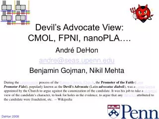
Devil’s Advocate View: CMOL, FPNI, nanoPLA…. Andr é DeHon andre@seas.upenn.edu Benjamin Gojman, Nikil Mehta.

E N D
Devil’s Advocate View:CMOL, FPNI, nanoPLA…. André DeHon andre@seas.upenn.edu Benjamin Gojman, Nikil Mehta During the canonization process of the Roman Catholic Church, the Promoter of the Faith (LatinPromotor Fidei), popularly known as the Devil's Advocate (Latin advocatus diaboli), was a canon lawyer appointed by the Church to argue against the canonization of the candidate. It was his job to take a skeptical view of the candidate's character, to look for holes in the evidence, to argue that any miracles attributed to the candidate were fraudulent, etc. -- Wikipedia
Case • Molecules are not miraculous. • Miracle of high density is exaggerated. • Miracle of low energy is a slight of hand. • Curse of variation falls on all who would dare reach the atomic-scale.
Two Ideas Benefits follow from two hypotheses: • Can fabricate parallel wires denser than arbitrary topology • Can place resistance-varying switch with quasi-non-volatile state in space of dense wire crossing • Hysteretic switching • No extra area to program Valid Prospects? “Let’s build regular architectures around resistive switches!”
Inquisition • What problem does CMOL/FPNI solve? • Is this the bottleneck to scaling?
Problem Solved? • What problem do these technology hypotheses address? • Density • (Economical) density 11 ITRS 2007 Execsum Table 1i; assume 4TR/gate
Unpack Assumptions • Previous table appears to assume • 100,000 F2 per “gate” in FPGA case • 250,000 F2 / 4-LUT × 2.5 gates/4-LUT • Plausible, conservative • 64 FCMOS2 per “gate” in CMOL case • assuming each buffer is a gate and buffer is 64F2 • This assumption is stated in FPGA2006 paper. • Optimistically small. …plausibly within factor of 2. • Ignores that most of these buffers will act as route through (provide no gates).
Right Problem? • Is logic density of gates the bottleneck in scaling? • Economical logic density? • Density of programmable gates?
What is the Scaling Bottleneck? • Density? • Delay? • Power Density? • Reliability? • Test and handling economics?
Methodology:Benchmark-Level Quantification • For following, map Toronto 20 benchmarks • 20 Largest MCNC benchmarks • Order of 10K gates each • (so think small cores) • Composite density/performance/energy • Includes overheads, route-through, fanout…
Density: Mapped LogicStrukov and Likharev FPGA2006 • Only about 1 in 4 “gates” used as logic • 775/4 ≈ 190 comparable to ASIC gate density
Density: Mapped Logic • PDC benchmark – 2 cases: • Conservative • (defective wires, stochastic assembly, lithographic support overhead) • Optimistic Extreme (ideal, no litho overhead)
How much density from nanowires? • Look at Fcmos=Fnano=22nm (Fcmos/Fnano largest) • 42 Mgates/cm2 • 20× better than CMOS FPGA • 5--20× worse than Fnano=3nm
Delay • Challenge has been to turn capacity (area) into performance • Linear scaling considered excellent • Something which is 10× denser • Better be less than 10× slower • E.g. we expect 10 cores running at 100MHz to run slower than 1 core running at 1GHz • If give up too much delay, no benefit.
Obtaining Performance • Highly Pipelined nanoPLA designs • Conservative (demonstrated tech.) • Ronxpoint=100KW, rSi=10-3W-cm, rNiSi=10-5W-cm • Only NiSi non-active areas Pipe delay stages = 452 Likharev only claim about 1GHz (unpipelined). (Nanoarch2007)
Power Density • Clock rates stopped scaling due to power density • We can already fabricate more transistors than we can afford to activate. • Looking at gate capacitance alone (45nm) • (highly optimistic, no wire) • 6×10-17 J/Tr/op (Vdd=1V) • ×700MTr/cm2 • ×10GHz • = 420W/cm2 (3000W/cm2 at 22nm, Vdd=0.7V)
Power Density: Quantitative • What if we run them at full speed? CMOL dodge here is assuming Vdd=0.3V.
Power Density: Quantitative • What can we use at 100W/cm2?
Energy per Gate Evaluation (CMOL) 40,000—60,000 kTln(2) per gate at T=300K Cg,total (FO4)≈0.18fF 22nm CMOS W=2Fcmos Vdd=0.65 13,000 kTln(2) for T=300K Vdd=0.3 2,800 kTln(2)
Reliability:Can we lower the voltage? • Lower voltage • Lower energy/op • Less headroom for Vt variation • More leakage, lower performance • More bad parts compensate with sparing • Subthreshold Operation • Trade energy for performance • Fewer electrons defining state • Higher susceptibility to transient upset • Thermal, shot ionizing particles.
Upset Rates • Lower Voltage to achieve 100W/cm2 • Assume (10% activity) • V=176mV (1GHz, 22nm,3Ggates/cm2) • 1cm2 FIT Rates • Thermal 10-6233 [calc. based on Kish PhysLetA 2002] • Shot 10-700 [calc. based on Kish FNL2004] • Increase in upset rate V=700mV to 176mV • Ionizing Particle upsets increase 20-100× • [calc. based on Cohen IEDM1999, Degalahal ISQED2004] • Lack information for absolute grounding. Suggestions for better sources for reliability calculations appreciated.
Variation and Yield • Are voltages plausible given variation? • ASIC: optimistic bound • Require devices have 0<Vth<Vdd • Vth(1-ks)>0 and Vth(1+ks)<Vdd • Say Vth=Vdd/2 • For 3Ggates k≈6-7 s≤14% • With ability to avoid gates • Let valid range be +/-1s 68% of devices • Good buffer 46% of time density impact ~ 2 • Tolerates much larger variation
Penn IC Group have ideas to address. Testing and Handling • Highly defective • nanoPLA/CMOL/FPNI exploit component-specific mapping to tolerate • Demands painful paradigm shift • Assume can run mapping in 4 hrs on 250W workstation • 1KWhr/chip x $0.15/1KWhr = $0.15 • (2000 Wafers/day x 675 dies/wafer) / 6 = 225,000 Workstations • But those live at customer site… • not to mention handling ….
Bottleneck Conclusion • Work in an E-D-A-Relability trade space • Density is not the clear limiter • Big hope is to trade this density to address other problems • Power density • Energy • Variation • Reliability
Additional Assumptions By Style • CMOL • Pins above metallization • FPNI • Nanoscale alignment of lithographic contacts • Not just parallel lines • Kuekes says litho rotated (7/12) • nanoPLA • Relatively reliable assembly of large number of NWs • Reasonably controlled production of doped (coded) NWs
Inquisition Report • If believed could achieve roadmap • CMOS ASICs provide density @ higher performance • If need fine-grained programmability • Variation • Economics force few unique platforms • …benefit from inexpensive programmability • 100-400× density benefit • Plausible performance (as far as energy allows) • Maybe 1GHz instead of 10GHz (1/10th the speed) • Reduce energy through sparing/repair to contain variation • Will cost post-fabrication handling
Summing Up • Molecules are not miraculous. • Miracle of high density is exaggerated. • Non-existent compared to ASIC • Closer to 2 orders of magnitude than 3 for FPGA • Miracle of low energy is a slight of hand. • Comes with a curse on reliability. • Curse of variation falls on all who would dare reach the atomic-scale. • …grace of repair may be all that saves us • Not unique to CMOL • Small switches may help.
References • nanoPLA articles http://www.seas.upenn.edu/~andre/sublithographic.html • Likharev, “Hybrid CMOS/Nanoelectronic Circuits(CMOL, FPNI, etc.)”,White Paper for ITRS ERD Working Group 2008 • Strukov and Likharev, FPGA 2006 • Likharev and Strukov, Nanoarch 2007
Simple Nanowire-Based PLA NOR-NOR = AND-OR PLA Logic DeHon&Wilson FPGA 2004
Interconnected nanoPLA Tile DeHon JETC 2005
Transfer aligned NWs to patterned substrate Transfer second layer at right angle + Langmuir-Blodgett (LB) transfer • Can transfer tight-packed, aligned SiNWs onto surface • Maybe grow sacrificial outer radius, close pack, and etch away to control spacing Whang, Nano Letters 2003 v7n3p951