Download
1 / 22
220 likes | 336 Views
Non-Contacting Eddy Current Conductivity Sensor for Measuring Doped Silicon Wafers For MEMS Applications. A Finite Element Analysis ( FEA ) using flexPDE. Craig E. Nelson - Consultant Engineer. Purpose of the Numerical Experiment:

E N D
Non-Contacting Eddy Current Conductivity Sensor for Measuring Doped Silicon Wafers For MEMS Applications A Finite Element Analysis ( FEA ) using flexPDE Craig E. Nelson - Consultant Engineer
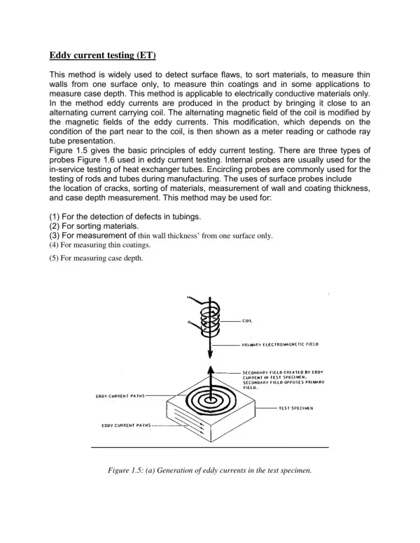
Purpose of the Numerical Experiment: The purpose of this numerical experiment is to learn something about the electromagnetic fields, induced currents and absorbed power in and around a silicon wafer placed above a “cup core” coil excited at an RF frequency. For this analysis, I used an excitation frequency of 5 MHz. However, because I wanted the option of exciting the system at substantially higher frequencies, I employed the full blown Helmholtz wave equation formulation for media that are specified by their permeability, permittivity and conductivity. Because the excitation is sinusoidal, the various field parameters are complex valued. Using the wave equation approach, the excitation frequency in the model could be raised high enough for radiation of energy from the system to occur … and … be accurately evaluated. I was interested in this from a “how much EMI shielding do I need” and “will the shielding lower the performance of the sensor” point of view.
Silicon Wafer to be Measured Ferrite Cup Core Center Hole in Cup Core Magnet Coil Line of Symmetry Solution Domain
Silicon Wafer to be Measured Ferrite Cup Core Center Hole in Cup Core Line of Symmetry Magnet Coil Analysis Grid
Vector Magnetic Potential field – Azimuthal - Real Component {This field effectively shows the magnetic lines of flux}
Current Density on Wafer Center Plane – Azimuthal - Real Component
Summary and Conclusions A finite element model has been developed that allows insight into the nature and magnitude of electromagnetic fields, induced currents and absorbed power in a silicon wafer placed above a “cup core” coil excited at an arbitrary RF frequency. The model uses the Helmholtz “full wave” formulation which allows analysis of radiation from the system. This model could be developed in many further ways.