Download
1 / 12
130 likes | 211 Views
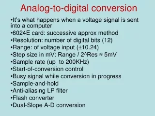
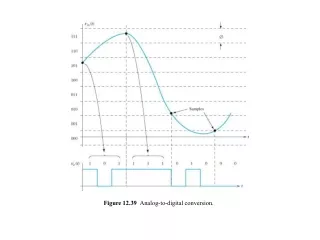
Figure 12.39 Analog-to-digital conversion. Figure 12.40 The DAC output is a staircase approximation to the original signal. Filtering removes the sharp corners. ( Note: In addition to smoothing, the filter delays the signal. The delay is not shown.). 7 Δ. 6 Δ. 5 Δ. 4 Δ. 3 Δ. 2 Δ.

E N D
Figure 12.40 The DAC output is a staircase approximation to the original signal. Filtering removes the sharp corners. (Note: In addition to smoothing, the filter delays the signal. The delay is not shown.)
7Δ 6Δ 5Δ 4Δ 3Δ 2Δ 1Δ 0Δ Figure 12.49 Output versus input for a 3-bit flash A/D converter
DNL (differential nonlinearity) and INL (integral nonlinearity)
Figure 12.41 Circuit symbol for a digital-to-analog converter.
Figure 12.42 DACs can be implemented using a weighted-resistance network. (Note: If di = 1, the corresponding switch is to the right-hand side. For di = 0, the i th switch is to the left-hand side.)
Figure 12.43 An R -- 2R ladder network. The resistance seen looking into each section is 2R. Thus, the reference current splits in half at each node.
Figure 12.45 Parallel, simultaneous, or flash A/D conversion.
Initially, all bits are set to 0 In step 1, the control logic sets MSB to 1 and if the comparator output is high, MSB is set back to 0, otherwise MSB remains 1 The process is repeated for the next bit. After n steps, the process is complete, and the input to the DAC is the digital code for the analog input.
Oversampling A/D converters E(n)=Y(n)-X(n) is defined as quantization noise, Y(n) is the quantized output and X(n) is the input. E(n) is between (-∆/2, ∆/2) Where ∆ is the quantization level. E(n) is typically approximated as an independent uniformly distributed white noise and its power spectral density is k= , fs is the sampling frequency. Therefore, increase the fs relative to the signal bandwidth will give higher resolution than Nyquist sampling converters. Even further, if oversampling is combined with noise shaping, such as in a Sigma-Delta A/D converter, then the resolution could be even higher.