Download
1 / 1
10 likes | 190 Views
Electron-Phonon Scattering in NW FETs Mathieu Luisier and Gerhard Klimeck PRB 80, 155430 (2009). Objective:

E N D
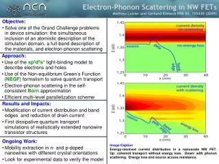
Electron-Phonon Scattering in NW FETsMathieu Luisier and Gerhard Klimeck PRB 80, 155430 (2009) Objective: • Solve one of the Grand Challenge problems in device simulation: the simultaneous inclusion of an atomistic description of the simulation domain, a full-band description of the materials, and electron-phonon scattering Approach: • Use of the sp3d5s* tight-binding model to describe electrons and holes • Use of the Non-equilibrium Green’s Function (NEGF) formalism to solve quantum transport • Electron-phonon scattering in the self-consistent Born approximation • Efficient multi-level parallelizationscheme Results and Impacts: • Modification of current distribution and band edges and reduction of drain current • First dissipative quantum transport simulations of realistically extended nanowire transistor structures Ongoing Work: • Mobility extraction in n- and p-doped nanowires with different crystal orientations • Look for experimental data to verify the model Image Caption Energy-resolved current distribution in a nanoscaleNW FET. Up: coherent transport without energy loss. Down: with phonon scattering. Energy loss and source access resistance.