Download
1 / 33
340 likes | 514 Views
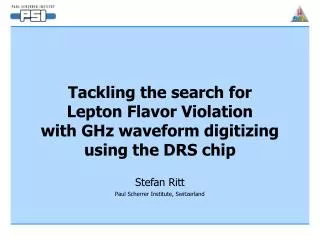
Application of the DRS Chip for Fast Waveform Digitizing. Stefan Ritt Paul Scherrer Institute, Switzerland. Question ?. 4 channels 5 GSPS 1 GHz BW 8 bit (6-7) 15k$. 4 channels 5 GSPS 1 GHz BW 11.5 bits 1k$ USB Power. Switched Capacitor Array. 0.2-2 ns.

E N D
Application of the DRS Chip for Fast Waveform Digitizing Stefan Ritt Paul Scherrer Institute, Switzerland
Question ? 4 channels 5 GSPS 1 GHz BW 8 bit (6-7) 15k$ 4 channels 5 GSPS 1 GHz BW 11.5 bits 1k$ USB Power TIPP09 Tsukuba
Switched Capacitor Array 0.2-2 ns Inverter “Domino” ring chain IN Waveform stored Out FADC 33 MHz Clock Shift Register “Time stretcher” GHz MHz TIPP09 Tsukuba
Switched Capacitor Array • Cons • No continuous acquisition • Limited sampling depth • Nonlinear timing • Pros • High speed (6 GHz) high resolution (11.5 bit resol.) • High channel density (9 channels on 5x5 mm2) • Low power (10-40 mW / channel) • Low cost (~ 10$ / channel) Dt Dt Dt Dt Dt Goal: Minimize Limitations TIPP09 Tsukuba
DRS4 • Designed for the MEGexperiment at PSI,Switzerland • UMC 0.25 mm 1P5M MMC process(UMC), 5 x 5 mm2, radiation hard • 8+1 ch. each 1024 cells • Differential inputs,differential outputs • Sampling speed 500 MHz … 6 GHz,PLL stabilized • Readout speed 30 MHz, multiplexedor in parallel TIPP09 Tsukuba
How to minimize dead time ? • Fast analog readout: 30 ns / sample • Parallel readout • Region-of-interestreadout • Simultaneouswrite / read AD9222 12 bit 8 channels TIPP09 Tsukuba
ROI readout mode delayed trigger stop normal trigger stop after latency stop Trigger Delay 33 MHz e.g. 100 samples @ 33 MHz 3 us dead time 300,000 events / sec. readout shift register Patent pending! TIPP09 Tsukuba
Daisy-chaining of channels Domino Wave Domino Wave clock clock enable input enable input 1 Channel 0 0 Channel 0 enable input enable input 0 Channel 1 1 Channel 1 Channel 2 0 Channel 2 1 Channel 3 Channel 3 1 0 Channel 4 Channel 4 0 1 Channel 5 Channel 5 1 0 Channel 6 Channel 6 0 1 Channel 7 Channel 7 1 0 DRS4 can be partitioned in: 8x1024, 4x2048, 2x4096, 1x8192 cellsChip daisy-chaining possible to reach virtually unlimited sampling depth TIPP09 Tsukuba
readout Channel 0 1 Channel 0 1 0 1 Channel 1 Channel 1 Channel 2 Simultaneous Write/Read FPGA 0 Channel 0 0 Channel 1 8-foldanalog multi-eventbuffer Channel 2 0 Channel 3 0 Channel 4 0 Channel 5 0 Channel 6 0 Channel 7 0 Expected crosstalk ~few mV TIPP09 Tsukuba
DRS4 MUX Trigger an DAQ on same board • Using a multiplexer in DRS3, input signals can simultaneously digitized at 65 MHz and sampled in the DRS • FPGA can make local trigger(or global one) and stop DRSupon a trigger • DRS readout (6 GHz samples)though same 8-channel FADCs global trigger bus trigger FPGA DRS FADC12 bit 65 MHz analog front end LVDS SRAM “Free” local trigger capability without additional hardware TIPP09 Tsukuba
DRS4 Performance Test Results
Bandwidth • Bandwidth is determined by bond wire and internalbus resistance/capacitance: • 850 MHz (QFP), 950 MHz (QFN), ??? (flip-chip) QFP package finalbus width 850 MHz (-3dB) Simulation Measurement TIPP09 Tsukuba
Timing jitter • Inverter chain has transistor variations Dti between samples differ “Fixed pattern aperture jitter” • “Differential temporal nonlinearity” TDi= Dti – Dtnominal • “Integral temporal nonlinearity”TIi = SDti – iDtnominal • “Random aperture jitter” = variation of Dti between measurements Dt1 Dt2 Dt3 Dt4 Dt5 TD1 TI5 TIPP09 Tsukuba
Fixed jitter calibration • Fixed jitter is constant over time, can be measured and corrected for • Several methods are commonly used • Most use sine wave with random phase and correct for TDi on a statistical basis TIPP09 Tsukuba
Sine Curve Fit Method i yji : i-th sample of measurement j aj fj ajoj : sine wave parameters bi : phase error fixed jitter • “Iterative global fit”: • Determine rough sine wave parameters for each measurement by fit • Determine bi using all measurements where sample “i” is near zero crossing • Make several iterations j S. Lehner, B. Keil, PSI TIPP09 Tsukuba
Fixed Pattern Jitter Results • TDi typically ~50 ps RMS @ 5 GHz • TIi goes up to ~600 ps • Jitter is mostly constant over time, measured and corrected • Residual random jitter 3-4 ps RMS TIPP09 Tsukuba
Applications of the DRS4 Chip What can we do with this technology?
Baseline Restoration Transimpedance Preamplifier PMT/APD Wire FADC 5 GHz12 bit Digital Processing Flash ADC Technique FADC Q-sensitive Preamplifier 60 MHz12 bit Shaper PMT/APD Wire Amplitude TDC Time • Shaper is used to optimize signals for “slow” 60 MHz FADC • Shaping stage can only remove information from the signal • Shaping is unnecessary if FADC is fast enough • All operations (CFD, optimal filtering, integration) can be done digitally TIPP09 Tsukuba
How to measure best timing? Simulation of MCP with realistic noise and different discriminators J.-F. Genat et al., arXiv:0810.5590 (2008) TIPP09 Tsukuba
On-line waveform display S848 PMTs “virtual oscilloscope” template fit click pedestal histo TIPP09 Tsukuba
Pulse shape discrimination Example: a/g source in liquid xenon detector (or: g/p in air shower) a g Leading edge Decay time AC-coupling Reflections TIPP09 Tsukuba
t-distribution ta = 21 ns tg = 34 ns Waveforms can be clearly distinguished a g TIPP09 Tsukuba
Template Fit • Determine “standard” PMT pulse by averaging over many events “Template” • Find hit in waveform • Shift (“TDC”) and scale (“ADC”)template to hit • Minimize c2 • Compare fit with waveform • Repeat if above threshold • Store ADC & TDC values pb Experiment 500 MHz sampling Pile-up can be detected if two hits are separated in time by ~rise time of signal TIPP09 Tsukuba
Timing Big Systems I Jitter: 400 fs LMK03000 Clock Conditioner(National Semiconductor) GlobalClock ~20 MHz ReferenceClock forDRS4 PLL 2.5 MHz ReferenceClock fortiming channel TIPP09 Tsukuba
Timing Big Systems II Experiment wide global clock DRS4Chip LMK03000 PLL Domino Wave Channel 0 Channel 1 • Global clock locks all Domino Wavesto same frequency and phase • Residual random jitter: 25 ps • Even better timing can be obtained by clock sampling • MEG Experiment: Single LVDSclock distributed over 9 VMEcrates Channel 2 Channel 3 Channel 4 Channel 5 Channel 6 Channel 7 Channel 8 TIPP09 Tsukuba
Experiments using DRS chip MEG 3000 channels DRS2 upgraded to DRS4 soon MAGIC-II 400 channels DRS2 BPM for XFEL@PSI 1000 channels DRS4 (planned) PET MACE (India) 400 channels DRS4 (planned) TIPP09 Tsukuba
32-channel 65 MHz/12bit digitizer “boosted” by DRS4 chip to 5 GHz Availability • DRS4 can be obtained from PSI on a “non-profit” basis • Delivery “as-is” • Costs ~ 10-15 USD/channel (1000-1500 JPY) • USB Evaluation board as reference design • VME boards from industry in 2009 TIPP09 Tsukuba
Conclusions • Fast waveform digitizing with SCA chips will have a big impact on experiments in the next future • DRS4 has 6 GHz, 1024 sampling cells per channel, 9 channels per chip, 11.5 bit vertical resolution, 4 ps timing resolution • ~4000 DRS channels already used in several experiments, hope that other experiments can benefit from this technology http://drs.web.psi.ch TIPP09 Tsukuba
Datasheet http://drs.web.psi.ch/datasheets TIPP09 Tsukuba
Signal-to-noise ratio (DRS3!) • “Fixed pattern” offset error of 5 mV RMScan be reduced to 0.35 mV by offsetcorrection in FPGA • SNR: • 1 V linear range / 0.35 mV = 69 dB (11.5 bits) Offset Correction TIPP09 Tsukuba
G. Varner et al., Nucl.Instrum.Meth. A583, 447 (2007) Interleaved sampling 6 GSPS * 8 = 48 GSPS delays (167ps/8 = 21ps) Possible with DRS4 if delay is implemented on PCB TIPP09 Tsukuba
Constant Fraction Discr. Delayed signal Inverted signal Sum Clock 12 bit Latch Latch Latch Latch + Latch Latch S + <0 & MULT 0 TIPP09 Tsukuba