Download
1 / 27
270 likes | 418 Views
Fast Waveform Digitizing in Radiation Detection using Switched Capacitor Arrays. Stefan Ritt Paul Scherrer Institute, Switzerland. Question ?. 4 channels 5 GSPS 1 GHz BW 8 bit (6-7) 15k$. 4 channels 5 GSPS 1 GHz BW 11.5 bits 1k$ USB Power. The need for speed. Q-ADC.

E N D
Fast Waveform Digitizing in Radiation Detection using Switched Capacitor Arrays Stefan Ritt Paul Scherrer Institute, Switzerland
Question ? 4 channels 5 GSPS 1 GHz BW 8 bit (6-7) 15k$ 4 channels 5 GSPS 1 GHz BW 11.5 bits 1k$ USB Power CMOS ET Vancouver
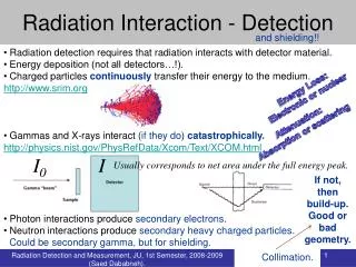
The need for speed Q-ADC • Traditional technique • Gated charge ADCs • Constant Fraction Disc. • Time-to-Digital Conv. • High rate applications • Pile-up becomes an issue Waveform digitizing • Issues: Limited speed andresolution • High channel counts • Power consumption • FADC Costs Det chan TDC Disc. Trigger FADC Det chan Needed: >3 GSPS 12 bit hits Moving average baseline CMOS ET Vancouver
Switched Capacitor Array 0.2-2 ns Inverter “Domino” ring chain IN Waveform stored Out FADC 33 MHz Clock Shift Register “Time stretcher” GHz MHz CMOS ET Vancouver
DRS4 • Designed for the MEGexperiment at PSI,Switzerland • UMC 0.25 mm 1P5M MMC process(UMC), 5 x 5 mm2, radiation hard • 8+1 ch. each 1024 cells • Differential inputs,differential outputs • Sampling speed 700 MHz … 5 GHz,PLL stabilized • Readout speed 30 MHz, multiplexedor in parallel CMOS ET Vancouver
Comparison with other chips CMOS ET Vancouver
Switched Capacitor Array • Pros (DRS4 chip) • High speed (5 GHz) high resolution (11.5 bit resol.) • High channel density (9 channels on 5x5 mm2) • Low power (10-40 mW / channel) • Low cost (~ 10$ / channel) • Cons • No continuous acquisition • Limited sampling depth • Nonlinear timing Dt Dt Dt Dt Dt Goal: Minimize Limitations CMOS ET Vancouver
How to minimize dead time ? • Fast analog readout: 30 ns / sample • Parallel readout • Region-of-interestreadout • Simultaneouswrite / read AD9222 12 bit 8 channels CMOS ET Vancouver
ROI readout mode delayed trigger stop normal trigger stop after latency stop Trigger Delay 33 MHz e.g. 100 samples @ 33 MHz 3 us dead time 300,000 events / sec. readout shift register Patent pending! CMOS ET Vancouver
Daisy-chaining of channels Domino Wave Domino Wave clock clock enable input enable input 1 Channel 0 0 Channel 0 enable input enable input 0 Channel 1 1 Channel 1 Channel 2 0 Channel 2 1 Channel 3 Channel 3 1 0 Channel 4 Channel 4 0 1 Channel 5 Channel 5 1 0 Channel 6 Channel 6 0 1 Channel 7 Channel 7 1 0 DRS4 can be partitioned in: 8x1024, 4x2048, 2x4096, 1x8192 cellsChip daisy-chaining possible to reach virtually unlimited sampling depth CMOS ET Vancouver
readout Channel 0 1 Channel 0 1 0 1 Channel 1 Channel 1 Channel 2 Simultaneous Write/Read FPGA 0 Channel 0 0 Channel 1 8-foldanalog multi-eventbuffer Channel 2 0 Channel 3 0 Channel 4 0 Channel 5 0 Channel 6 0 Channel 7 0 Expected crosstalk ~few mV CMOS ET Vancouver
G. Varner et al., Nucl.Instrum.Meth. A583, 447 (2007) Interleaved sampling 6 GSPS * 8 = 48 GSPS delays (167ps/8 = 21ps) Possible with DRS4 if delay is implemented on PCB CMOS ET Vancouver
DRS4 MUX Trigger and DAQ on same board • Using a multiplexer in DRS4, input signals can simultaneously digitized at 65 MHz and sampled in the DRS • FPGA can make local trigger(or global one) and stop DRSupon a trigger • DRS readout (5 GHz samples)though same 8-channel FADCs global trigger bus trigger FPGA DRS FADC12 bit 65 MHz analog front end LVDS SRAM “Free” local trigger capability without additional hardware CMOS ET Vancouver
Performance of SCA Chips Test Results
Bandwidth • Passive Input: Bandwidth is determined by bond wire and internal bus resistance/capacitance: • 850 MHz (QFP), 950 MHz (QFN), ??? (flip-chip) • Active Inputs: ~300 MHz with currentCMOS technology (MATACQ) • Near future: 130 nm technologymight improve this slightly QFP package 850 MHz (-3dB) Measurement CMOS ET Vancouver
Timing jitter • Inverter chain has transistor variations Dti between samples differ “Fixed pattern aperture jitter” • “Differential temporal nonlinearity” TDi= Dti – Dtnominal • “Integral temporal nonlinearity”TIi = SDti – iDtnominal • “Random aperture jitter” = variation of Dti between measurements Dt1 Dt2 Dt3 Dt4 Dt5 TD1 TI5 CMOS ET Vancouver
Fixed jitter calibration • Fixed jitter is constant over time, can be measured and corrected for • Several methods are commonly used • Most use sine wave with random phase and correct for TDi on a statistical basis CMOS ET Vancouver
Fixed Pattern Jitter Results • TDi typically ~50 ps RMS @ 5 GHz • TIi goes up to ~600 ps • Jitter is mostly constant over time, measured and corrected • Residual random jitter (RMS) • 25 ps MATACQ • 10 ps Labrador • 3-4 ps DRS4 SCA technology can replace high resolution TDCs CMOS ET Vancouver
Applications of SCA Chips What can we do with this technology?
On-line waveform display S848 PMTs “virtual oscilloscope” template fit click pedestal histo CMOS ET Vancouver
Pulse shape discrimination Example: a/g source in liquid xenon detector (or: g/p in air shower) a g Leading edge Decay time AC-coupling Reflections CMOS ET Vancouver
t-distribution ta = 21 ns tg = 34 ns Waveforms can be clearly distinguished a g CMOS ET Vancouver
Template Fit • Determine “standard” PMT pulse by averaging over many events “Template” • Find hit in waveform • Shift (“TDC”) and scale (“ADC”)template to hit • Minimize c2 • Compare fit with waveform • Repeat if above threshold • Store ADC & TDC values pb Experiment 500 MHz sampling Pile-up can be detected if two hits are separated in time by ~rise time of signal CMOS ET Vancouver
Experiments using DRS chip MEG 3000 channels DRS4 MAGIC-II 400 channels DRS2 BPM for XFEL@PSI 1000 channels DRS4 (planned) PET MACE (India) 400 channels DRS4 (planned) CMOS ET Vancouver
Datasheet http://drs.web.psi.ch/datasheets CMOS ET Vancouver
Evaluation Board • DRS4 can be obtained from PSI on a “non-profit” basis • Delivery “as-is” • Costs ~ 15-20 CAN$/chn • USB Evaluation board as reference design • Anybody wants to build a pocket scope? CMOS ET Vancouver
Conclusions • This is Exciting Stuff! • DRS4 has 6 GHz, 1024 sampling cells per channel, 9 channels per chip, 11.5 bit vertical resolution, 4 ps timing accuracy, other chips similar • More development in the pipeline • Fast waveform digitizing with SCA chips will have a big impact on particle detection in the next future • Other fields should benefit from this development LABRADOR: http://www.phys.hawaii.edu/~idlab/ MATACQ: http://matacq.free.fr/ DRS4: http://drs.web.psi.ch CMOS ET Vancouver