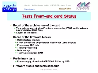
Tests Front-end card Status
200 likes | 225 Views
Detailed review of the design and testing components of the FPGA and interface test board architecture. Includes firmware block recall, power supply setup, clock tree configuration, and preliminary testing methodologies.

Tests Front-end card Status
E N D
Presentation Transcript
Tests Front-end card Status Recall of the architecture of the card Time adjustment , Analog Front-end mezzanine, FPGA and Interfaces, power supply, Clock Tree. Layout of the board. Recall of the firmware blocks USB interface module Clock divider and L0 generator module for Lemo outputs Processing ADC data Trigger processing Data storage Test value injection RAM Preliminary tests Power supply, download A3PE1500, Rd/wr by USB Firmware status and tests schedule LHCb upgrade meeting
Tests board architecture Tests board architecture Schedule for SPECS development Time adjustement and input/output of the board Analog Front-end mezzanine FPGA and Interfaces LHCb upgrade meeting
Time adjustment with delay chip and Input/Output (LEMO) CROC prototype tests : schedule Schedule for SPECS development More information on the clock tree slide ! Choice CERN / LAL by resistor • 3 Inputs (NIM translator) for A3PE FPGA • 3 Outputs (NIM translator) for A3PE FPGA • 1 Input (NIM translator) for AX FPGA • 1 Output (NIM translator) for AX FPGA • 1 Input Ext_Clk (NIM translator) for A3PE • 1 Output Ext_Clk (NIM translator) for A3PE LHCb upgrade meeting
Analog Front-end mezzanine CROC prototype tests : schedule Schedule for SPECS development • 8 x {ADC_Data Channel (12b)} • 8 x {Clk for ADC_Data Channel (LVDS)} • 2 x Global Clk (LVDS) • 4 Spare for A3PE • 4 Spare for AX500 • I2C • Reset • Parallel Bus • AVEE, DVDD, AVCC_1, AVCC_2 Foot print of Analog Mezzanine LHCb upgrade meeting
FPGA and Interfaces CROC prototype tests : schedule Schedule for SPECS development FPGA and Interfaces Flash Pro 4 to be used to programming A3PE device • A3PE1500 • AX500 (socket) • SPECS and USB Interface through A3PE • I2C Interface from A3PE to AX • JTAG download for A3PE • JTAG for AX : Silicon Explorer LHCb upgrade meeting
Tests board power supply CROC prototype tests : schedule Schedule for SPECS development P7V Regulator - 4913 AVCC_1 for Analog Mezza (+3 to +5V) Regulator - 4913 AVCC_2 for Analog Mezza (+3 to +5V) Regulator - 4913 DVDD for Analog Mezza (+2V5 to +3V3) VCC for board (+5V) Regulator - 4913 P3V3 for board (+3,3v) Regulator - 4913 (VccIO bank fixe) Regulator - 4913 P1V5 for FPGA core 1,5v < VccIOB_Var < +2,5v) Regulator - 4913 (VccIO bank variable) P2V5 for bank (+2,5v) Regulator - 4913 (VccIO bank LVDS) M7V Regulator - 7913 AVEE for Analog Mezza (-3 to -5V) Regulator - 7913 VEE for board (-5V) {NIM translators} • Lab. Power Supply input (+/- 7V) • 10 Radiation tolerance regulators ! ! LHCb upgrade meeting
Tests board Clock Tree CROC prototype tests : schedule Schedule for SPECS development • Each FPGA receive 2 adjustable Clock (LVDS) • Analog mezzanine receive also 2 adjustable Clock (LVDS) • Each ADC_Channel receive 1 Clock (LVDS) LHCb upgrade meeting
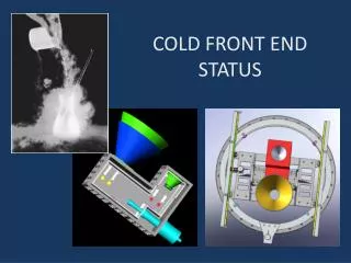
Layout of the board USB IN / OUT (NIM) SPEC Mezzanine Delay Chip A3PE1500 REGULATORS Analog Mezzanine 120mm x 120mm AX500 Board size : 305 mm x 155 mm 10 layers "LAL Support" for AX 500 LHCb upgrade meeting
Test_FE Board A3PE1500 SPEC Mezzanine LHCb upgrade meeting
Recall of the firmware blocks All Blocks inside A3PE1500 in Verilog language • USB interface module (Jihane’s code) • Clock divider and trigger generator module for Lemo outputs • (according Olivier’s code APA300 for CROC) • Processing ADC data (according Christophe’s code AX250) • Trigger processing • Data storage • Test value injection RAM LHCb upgrade meeting
A3PE firmware blocks : USB interface module • USB interface module • USB Interface standard module • I2C modules (x4) FT245 side User side Sda USB / I2C module Delay chip LAL Scl (x3) SubAdd[6..0] USB_Data[7..0] USB Interface Standard module UserData[7..0] Sda USB / I2C module RXF Delay chip CERN N_Write Scl (x3) RD N_Read N_Sync TXE Sda USB / I2C module AX500 WR Scl Interrupt Clk USB / I2C module Sda Analog mezzanine N_Reset Scl LHCb upgrade meeting
A3PE firmware blocks : Clockdivider and trigger generator • Clock divider • 50 ns to 0.4s (24 bits counter) • Internal Trigger With this module we can produce trigger (external trigger or software command) Tdelay (8bits) TL0 (16 bits) Registers loaded by USB or SPECS : Ndump (8bits) Nspy (8 bits) Registers loaded by USB or SPECS : LHCb upgrade meeting
A3PE firmware blocks : data processing • Processing ADC data • Re-synchronize ADC input • Dynamique pedestal subtraction • Suppression of low frequency noise • Trigger processing • Convert ADC data to 8 bit • Sent towards the TRIG-PGA AX500? RAM block 8 x 16 x 256 LHCb upgrade meeting
A3PE firmware blocks : RAM • Data storage (output buffer) before readout • 8 x 16 (12 used) x 256 • Read only by USB (first !) • Test value injection RAM • 8 x 16 (12 used) x 256 • Use of the RAM test describ in LHCb ECAL/ HCAL Front-End card • There exist different ways to use the RAM test: • - The standard one: the RAM address is increased every 25ns by the clock and the sequence of 256 addresses is initiated by the test-sequence signal, originating in the calibration command of the channel B and enabled by the corresponding status of an I2C register. The sequence ends up after 256 clock cycles. • - A variant with an enable loop bit loaded by I2C. In this case after the sequence initialisation the RAM address counter continues advancing and jumps automatically from address 255 to address 0. • - The L0 mode where the RAM address is incremented upon reception of each L0. The sequence can be terminated at 255 or looped as in case 2. • - Calibration mode where the RAM address is incremented upon reception of test sequence command. In this case by definition the system will loop after address 255. LHCb upgrade meeting
Preliminary tests • Power supply ok (AVcc_1, AVcc_2, AVee, ….) • Download A3PE1500 • A3P family require FlashPro 3 or 4 (new product !) • Problem with FlashPro Consol debug in progress with Actel • (“failed to load the programming file” {stp files}) • Rd / Wr register by USB inside A3P • USB interface Standard simulation ok • Used “test_245” by Chafik • Tests with 16 and 32 bits Rd/Wr register inside A3PE1500 to do Register 16 and 32 bits Rd / Wr FT245 side User side Sda USB / I2C module Delay chip LAL Scl (x3) SubAdd[6..0] USB Interface Standard module UserData[7..0] Sda RXF Delay chip CERN USB / I2C module N_Write Scl (x3) RD N_Read N_Sync TXE Sda USB / I2C module AX500 WR Scl Interrupt Clk Sda Analog mezzanine USB / I2C module N_Reset Scl LHCb upgrade meeting
Status of the firmware blocks • USB interface module (in progress Jihane + Olivier) • Clock divider and trigger generator module for Lemo outputs (to adapt from the CROC by Olivier) • Processing ADC data (in progress by Christophe) • Data storage (to do) • Test value injection RAM(to do) All Blocks inside A3PE1500 in Verilog language LHCb upgrade meeting
Tests schedule (optimistic !) April May June July - August September PCB Manufacturing (delayed !) Cabling (2 boards) (delayed !) 5 PCB Tests & firmware Holiday 1 operationalboard to "Barcelona team " 1board with Power and Clock to "Barcelona team " Nbre de PCB LHCb upgrade meeting
SPARE LHCb upgrade meeting
SPARE LHCb upgrade meeting
SPARE LHCb upgrade meeting