Download
1 / 9
90 likes | 104 Views
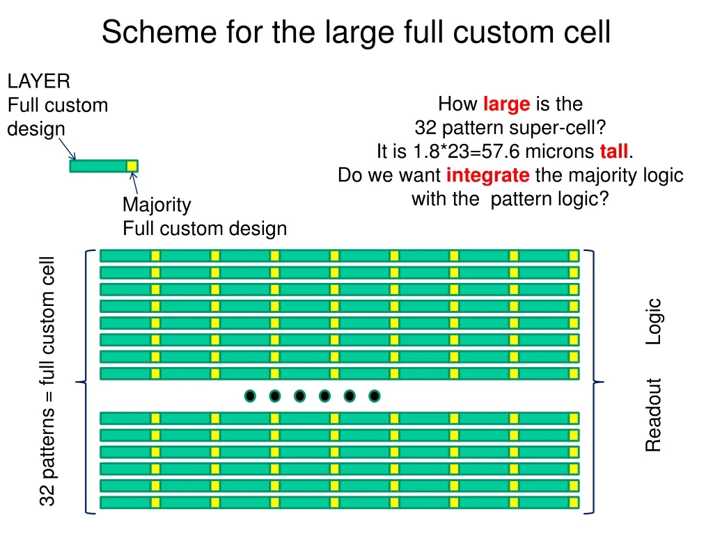
Scheme for the large full custom cell. LAYER Full custom design. How large is the 32 pattern super-cell? It is 1.8*23=57.6 microns tall . Do we want integrate the majority logic with the pattern logic?. Majority Full custom design. Readout Logic.

E N D
Scheme for the large full custom cell LAYER Full custom design How large is the 32 pattern super-cell? It is 1.8*23=57.6 microns tall. Do we want integrate the majority logic with the pattern logic? Majority Full custom design Readout Logic 32 patterns = full custom cell
& pattern organization in the 12 mm^2 -pad florplanning – power distribution 3 .46 mm ? How many Super-cells in a column? How much Space for readout? 3.46 mm ? Two faced pattern columns with readout in the middle How many couples of colums of Super-cells in X?
105 Vcc_IO • 106 NC • 107 OPcode3 • 108 OPcode2 • 109 Bus1_7 • 110 Bus1_6 • 111 Bus1_5 • 112 Bus1_4 • 113 Bus1_3 • 114 Bus1_2 • 115 Bus1_1 • 116 Bus1_0 • PattB0 • gnd • 119 pattB1 • 120 PattB2 • Vcc_IO • Debug_2 • 123 Debug_1 • 124 pattB3 • 125 pattB4 • 126 pattB5 • 127 pattB6 • 128 pattB7 • 129 pattB8 • 130 Vcc_IO • 131 gnd • 132 pattB9 • 133 pattB10 • 134 pattB11 • 135 pattB12 • 136 pattB13 • 137 pattB14 • 138 debug_0 • vcc_core • Vcc_IO • 141 pattB15 • 142 Bu3_0 • 143 gnd • 144 WiredDA_low • 145 Da_out • 146 Bus3_1 • 147 Bus3_2 • 148 Bus3_3 • 149 Bus3_4 • 150 Vcc_core • 151 SAin_Low • 152 Bus3_5 • 153 Bus3_6 • 154 pattB16 • 155 NC • 156 vcc_IO • 1 Gnd • 2 Bus7_11 • 3 SA_out • 4 Bus2_6 • 5 Bus2_5 • TDI • Bus2_4 • Bus2_3 • Bus2_2 • Bus2_1 • Bus2_0 • DA_in • Gnd • Vcc_core • Bus7_10 • Bus7_09 • Bus7_08 • Vcc_io • Bus7_07 • pattA13 • pattA12 • pattA11 • pattA10 • pattA9 • Gnd • Vcc_io • pattA8 • pattA7 • pattA6 • pattA5 • pattA4 • pattA3 • Vcc_io • Vcc_core • pattA2 • 36 Bus7_06 • 37 pattA1 • 38 gnd • 39 pattA0 • 40 Init_ev • 41 Bus0_0 • Bus0_1 • Bus0_2 • Bus0_3 • Bus0_4 • Bus0_5 • Bus0_6 • Bus0_7 • Opcode0 • Opcode1 • Gnd • Vcc_io • 105 Vcc_IO • 106 Gnd • 107 OPcode3 • 108 OPcode2 • 109 Bus1_7 • 110 Bus1_6 • 111 Bus1_5 • 112 Bus1_4 • 113 Bus1_3 • 114 B • 115 Bus1_1 • 116 Bus1_0 • 117 TMS • 118 PattB0 • 119 gnd • 120 pattB1 • 121BUS6_6 • 122 PattB2 • 123 Vcc_core • 124 Vcc_IO • 125 pattB3 • 126 pattB4 • 127 pattB5 • 128 pattB6 • 129 pattB7 • 130 pattB8 • 131 Vcc_IO • 132 gnd • pattB9 • pattB10 • 135 pattB11 • 136 pattB12 • 137 pattB13 • 138 Bus6_7 • 139 vcc_IO • 140 Bus6_8 • 141 Bus6_9 • 142 Bus6_10 • 143 vcc_core • 144 Gnd • 145 Da_out • 146 Bus3_0 • 147 Bus3_1 • 148 Bus3_2 • 149 Bus3_3 • 150 Bus3_4 • 151 TDO • 152 Bus3_5 • 153 Bus3_6 • 154 SA_in • 155 Bus6_11 • 156 Gnd • Vcc_IO • 103 Bus6_5 • Bus6_4 • Bus1_8 • Bus1_9 • 99 Bus1_10 • 98 Bus1_11 • 97 Bus1_12 • 96 Bus1_13 • 95 Bus1_14 • 94 Bus6_3 • 93 Bus6_2 • 92 Bus6_1 • 91 Gnd • 90 Bus6_0 • 89 • 88 Bus5_14 • 87 Bus5_13 • 86 Vcc_core • 85 Bus5_12 • 84 Bus5_11 • 83 Bus5_10 • 82 Bus5_9 • 81 Bus5_8 • 80 gnd • 79 clk • 78 clk • 77 gnd • 76 Bus5_7 • 75 Bus5_6 • 74 Bus5_5 • 73 Bus5_4 • 72 Bus5_3 • 71 Vcc_core • 70 Bus5_2 • 69 Bus5_1 • 68 Bus5_0 • 67 Bus7_00 • 66 gnd • 65 Bus7_01 • 64 Bus7_02 • 63 Bus7_03 • 62 Bus0_14 • 61 Bus0_13 • 60 Bus0_12 • 59 Bus0_11 • 58 Bus0_10 • 57 bus0_9 • 56 Bus0_8 • 55Bus7_04 • 54 Bus7_05 • 53 Vcc_io • Vcc_IO • Vcc_core • Bus3_7 • Vcc_IO • Bus3_8 • Bus3_9 • Bus3_10 • Bus3_11 • Bus3_12 • Bus3_13 • Bus3_14 • Bus6_12 • Bus6_13 • Gnd • Bus6_14 • 172 rev_en_low • Vcc_core • Bus4_14 • Bus4_13 • Bus4_12 • Bus4_11 • Bus4_10 • Bus4_09 • Bus4_8 • Bus4_7 • TCK • TCK • Bus4_6 • Bus4_5 • Bus4_4 • Bus4_3 • Bus4_2 • Bus4_1 • Bus4_0 • Vcc_core • rev_en_low • Bus7_14 • Gnd • Bus7_13 • Bus7_12 • Bus2_14 • Bus2_13 • Bus2_12 • Bus2_11 • Bus2_10 • Bus2_09 • bus2_08 • Vcc_IO • Bus2_07 • Vcc_core • Vcc_io • 1 Gnd • 2 pattA16 • 3 SA_out • 4 Bus2_6 • 5 Bus2_5 • TDI • TCK • Bus2_4 • Bus2_3 • Bus2_2 • Bus2_1 • DA_in • Gnd • Vcc_core • Bus2_0 • TMS • pattaA15 • Vcc_IO • pattA14 • pattA13 • pattA12 • pattA11 • pattA10 • pattA9 • Gnd • Vcc_io • pattA8 • pattA7 • pattA6 • pattA5 • pattA4 • pattA3 • Vcc_io • Vcc_core • pattA2 • 36 JTAG_RES • 37 pattA1 • 38 gnd • 39 pattA0 • 40 Init_ev • 41 Bus0_0 • Bus0_1 • Bus0_2 • Bus0_3 • Bus0_4 • Bus0_5 • Bus0_6 • Bus0_7 • Opcode0 • Vcc_IO • Gnd • Vcc_io External: new proposed pin-out symmetric for Mirroring around horizontal azis through 79-78 pins. Internally reported old chip pinout to evaluate movements Other side
Pattern bank Bus0[17:0] kill Bus1[17:0] Add encoder Bus2[17:0] Bus3[17:0] Bus4[17:0] Bus5[17:0] The CDF final AMchip architecture 14:0 →3x6=18 free 15 for new bus + 3 free 13:0 13:0 → 4 bits x 2=8 free
Summary of AMchip pinout Bus5[17-3:0] Bus0[17-3:0] Bus6-7[14:0] Bus0[17:0] Rev-en_ Debug[2:0] patt_add_a[17-4:0] patt_add_b[17-4:0] -1 Wired_da_ SA-out_ SA-in_ DA-in_ DA-out_ TOT FREE=30: 18+8+2+ 2NC pads -1 Opcode[3:0] Init clk
Pipelines of AM chips AMchip Control = GLUE add_in add_out Packaging chips together in the LAMB
add_out LAMB Bus3 Bus1 AM Bus4 AMTOP Bus5 Bus2 Bus0 add_in INDI Bus2 Bus0 Bus4 Bus5 AMBOTTOM REV_EN PAT_ADD_OUT [17:0] PAT_ADD_IN [17:0] Bus3 Bus1 REV_EN add_out
Case (1) Patt_add_in Patt_add_out up Patt_add_out Patt_add_in down Patt_add_in (or TDI, or SA_in…..) Patt_add_out (or TDO or SA_out….) up Case (2) Patt_add_in Patt_add_out Patt_add_in mirrored Patt_add_out Patt_add_in up
105 Vcc_IO • 106 NC • 107 OPcode3 • 108 OPcode2 • 109 Bus1_7 • 110 Bus1_6 • 111 Bus1_5 • 112 Bus1_4 • 113 Bus1_3 • 114 Bus1_2 • 115 Bus1_1 • 116 Bus1_0 • PattB0 • gnd • 119 pattB1 • 120 PattB2 • Vcc_IO • Debug_2 • 123 Debug_1 • 124 pattB3 • 125 pattB4 • 126 pattB5 • 127 pattB6 • 128 pattB7 • 129 pattB8 • 130 Vcc_IO • 131 gnd • 132 pattB9 • pattB10 • 134 pattB11 • 135 pattB12 • 136 pattB13 • 137 pattB14 • 138 debug_0 • vcc_core • Vcc_IO • 141 pattB15 • 142 Bu3_0 • 143 gnd • 144 WiredDA_low • 145 Da_out • 146 Bus3_1 • 147 Bus3_2 • 148 Bus3_3 • 149 Bus3_4 • 150 Vcc_core • 151 SAin_Low • 152 Bus3_5 • 153 Bus3_6 • 154 pattB16 • 155 NC • 156 vcc_IO • NC • 103 gnd • Opcode_1 • Bus1_8 • Bus1_9 • 99 Bus1_10 • 98 Bus1_11 • 97 Bus1_12 • 96 Bus1_13 • 95 Bus1_14 • 94 Bus1_15 • 93 Bus1_16 • 92 Bus1_17 • 91 Gnd • 90 Bus5_17 • 89 Bus5_16 • 88 Bus5_15 • 87 Bus5_14 • 86 Vcc_core • 85 Bus5_13 • 84 Bus5_12 • 83 Bus5_11 • 82 Bus5_10 • 81 Bus5_9 • 80 clk • 79 gnd • 78 Vcc_IO • NC • 76 Bus5_8 • 75 Bus5_7 • 74 Bus5_6 • 73 Bus5_5 • 72 Bus5_4 • 71 Vcc_core • 70 Bus5_3 • 69 Bus5_2 • 68 Bus5_1 • 67 Bus5_0 • 66 gnd • 65 Bus0_17 • 64 Bus0_16 • 63 Bus0_15 • 62 Bus0_14 • 61 Bus0_13 • 60 Bus0_12 • 59 Bus0_11 • 58 Bus0_10 • 57 bus0_9 • 56 Bus0_8 • 55 Vcc_core • 54 rev_en_low • 53 Vcc_io • TDO • gnd • Bus3_7 • pattB17 • Bus3_8 • Bus3_9 • Bus3_10 • Bus3_11 • Bus3_12 • Bus3_13 • Bus3_14 • Bus3_15 • Bus3_16 • Gnd • Bus3_17 • Bus4_17 • Vcc_core • Bus4_16 • Bus4_15 • Bus4_14 • Bus4_13 • Bus4_12 • Bus4_11 • Bus4_10 • Bus4_09 • Gnd p • Vcc_IO • Bus4_8 • Bus4_7 • Bus4_6 • Bus4_5 • Bus4_4 • Bus4_3 • Bus4_2 • Bus4_1 • Vcc_core • Bus4_0 • Bus2_17 • gnd • Bus2_16 • Bus2_15 • Bus2_14 • Bus2_13 • Bus2_12 • Bus2_11 • bus2_10 • Bus2_09 • Bus2_08 • Bus2_07 • Vcc_core • Vcc_IO OLD Pin_out as in CDF AMchip03 The green pads are holes that can be filled by the 2 new bases. • 1 Gnd • 2 pattA16 • 3 SA_out • 4 Bus2_6 • 5 Bus2_5 • TDI • TCK • Bus2_4 • Bus2_3 • Bus2_2 • Bus2_1 • DA_in • Gnd • Vcc_core • Bus2_0 • TMS • pattaA15 • Vcc_IO • pattA14 • pattA13 • pattA12 • pattA11 • pattA10 • pattA9 • Gnd • Vcc_io • pattA8 • pattA7 • pattA6 • pattA5 • pattA4 • pattA3 • Vcc_io • Vcc_core • pattA2 • 36 JTAG_RES • 37 pattA1 • 38 gnd • 39 pattA0 • 40 Init_ev • 41 Bus0_0 • Bus0_1 • Bus0_2 • Bus0_3 • Bus0_4 • Bus0_5 • Bus0_6 • Bus0_7 • Opcode0 • Vcc_IO • Gnd • Vcc_io