Download
1 / 33
340 likes | 653 Views
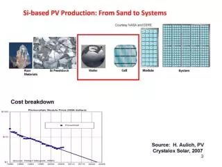
Chapter 7b Fabrication of Solar Cell. Different kind of methods for growth of silicon crystal. Electromagnetic Continuous Casting, not commercially available. Non-wafer Technologies. Specifications of PV Silicon Wafer. Cleaning and texturing.

E N D
Electromagnetic Continuous Casting, not commercially available
Cleaning and texturing • A layer with thickness of about 10 um has to be etched from both sides of wafers cut by wire saw. The damage removal etch is based on 20~30 wt% aqueous solution of NaOH or KOH heated to 80~90oC. • The silicon surface after saw damage etching is shiny and reflects more than 35% of incident light. • Random chemical texturing is used. Monocrystalline silicon substrate (100) can be textured by anisotropic etching at temperature of 70~80oC in a weak, usually 2wt%, solution of NaOH or KOH with addition of isopropanol.
texturing • This etch produces randomly distributed upside pyramids. However, It has problems of repeatability, lack of pyramid size control, and the presence of untextured regions. The important parameters are: adequate surface preparation, temperature control, mixing rate and isopropanol concentration. This requires the use of appropriate additives which enhance the pyramid nucleation process.
Junction formation, surface passivation and ARC • Highly doped P in 1020 atms-cm-3 • Typical emitter sheet resistance used in screen printing is between 40 and 60 Ohm/sq. • Front surface passivation: SiO2 • Antireflection coating: ZnS and MgF2, PECVD nitride (with n in 1.9~2.4) • Or Coating SiO2 thicker to 110 nm which serves as surface passivation and antireflection coating.
Front contact formation • Front contact formation: should have a large height-to-width ratio of finger metallization. After contact opening, metallization is obtained by a self-aligned plating process of nickel, copper, and a thin layer of silver. • In screen printing method, a stainless steel or polyester mesh screen stretched on a metal film frame is covered by a photo-emulsion layer. Openings- which define the front contact pattern- are photolithographically formed in the emulsion layer. Highly conductive silver paste is pushed by a squeegee through the openings in the screen onto substrates with well defined adjustable pressure.
Rear structure • Alloying a screen printed aluminum paste with silicon. Aluminum can form a eutectic alloy with silicon at a temperature of 577oC. During cooling down, the silicon recrystallizes and is doped with Al at its solubility limit creating a p+ back surface field (BSF) layer. A sufficient thickness of Al is required to achieve a significant contribution of Si in the formation of the liquid phase. Very low back surface recombination velocity (200cm/s) have been reported for thick screen printed and evaporated Al layers (at least 20 μm and 10 μm thick, respectively) fired at a temperature above 800oC.
Gettering – traps metal impurities by phosphorous diffusion • By phosphorous diffusion, metallic Impurity migration towards gettering sites takes place as a consequence of a large emission of Si interstitials due to the formation of SiP particles by heavy P-diffusion. Enhanced solubility of metallic impurities in such heavily P-diffused regions, and impurity segregation at Si3P4 precipitates lead to efficient gettering. P-diffusion can be performed prior to cell fabrication followed by the removal of the heavily diffused layers (pre-gettering), or a part of emitter formation depending on the optimal gettering conditions required for the material and on the costs involved.
Gettering by aluminum treatment • Formation of a p+/p high/low junction at the rear side of the cell by re-growth from a fast alloyed Al-Si melt is the most commonly used process for creating the back surface field. This has an additional advantage of bulk gettering by prolonged firing or by a thermal anneal after the initial firing. Fast alloying of screen printed Al-paste by firing, followed by the removal of excess aluminum and a subsequent thermal anneal for up to 1 h, resulted in a considerable enhancement in the bulk diffusion length in large area mc Si wafers.
EFG: Edge-defined film fed growth, a continuous production of a thin foil or sheet directly from the silicon melt. MIS: metal oxide semiconductor
Cell performance: 18% Reduce recombination velocity at the front contacts
Screen printing has the problems of large line width and contact resistance