Download
1 / 17
170 likes | 189 Views
This document provides the status of the test firmware architecture and board, including the schedule for SPECS development and details of the board size, components, and modules. It also outlines the steps for testing the firmware blocks and the progress made so far.

E N D
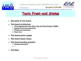
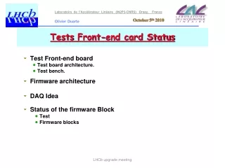
Tests Front-end card Status Test Front-end board Test board architecture. Test bench. Firmware architecture DAQ Idea Status of the firmware Block Test Firmware blocks LHCb upgrade meeting
Tests board architecture Tests board architecture Schedule for SPECS development Board size : 305 mm x 155 mm 10 layers IN / OUT (NIM) USB Delay Chip SPEC Mezzanine A3PE1500 REGULATORS AX500 Analog Mezzanine 120mm x 120mm "LAL Support" for AX 500 LHCb upgrade meeting
Test bench LHCb upgrade meeting
Firmware architecture (in A3PE1500) CROC prototype tests : schedule Schedule for SPECS development All Blocks inside A3PE1500 in Verilog language I2C1 (x3) Delay chip LAL USB / I2C module I2C2 (x3) Delay chip CERN USB / I2C module I2C3 USB / I2C module AX500 FPGA I2C4 USB / I2C module Analog mezzanine Step 1 : used the boardwith power supply and clock Ctrl USB Interface Status Register Tests register 16/32 bits Rd/Wr Step 2 : Add trigger and Delay Chip Ctrl Reset Register Ctrl Register Step 3 : Adddata processing and DAQ Global Clk (Diff 40 Mhz) In Ext Clk Clock Ctrl (10 Mhz) USB Clk Q : 40 Mhz SPECS Clk Out Ext Clk Trigger System Data FIFO/RAM Clock Divider • ADC Data • Test value injection ADC Data processing • Re-synchronize ADC Input • Dynamique pedestral subtraction Version : 08/01/2020 06:09 LHCb upgrade meeting
DAQ Idea … • Inside A3PE1500 • 60 blocks of 4608 Bit • For DAQ • 12 x 3 Blocks RAM to ADC data FIFO • 2 Blocks RAM to enable ADC data Ctrl_Register (16b) 1 0 Start acquisition (ADC running) • DAQ sequence • Load RAM sequence • USB Interface write the start_acquisition bit in the Ctrl_Register • ADC running • ADC data are writing in FIFO • When the FIFO is full we write FIFO_full bit in the Status_register • The PC scrutinize the status register and when the FIFO_full bit is high the USB read the FIFO • When the FIFO is empty we can start new acquisition USB Interface FIFO (18 x 768) To One ADC Channel 12 ADC Data input FIFO Empty 3 x RAMBlock of 18 x 256 FIFO Full PC 1 Status_Register (16b) Enable ADC RAM / FIFO Block for all channels 8 O_Enable ADC Channels or NIM connector (8 x 768) A3PE Firmware LHCb upgrade meeting
Tests Status ok • Download A3PE1500 with FlashPro 4 • (Problem solved) • Rd / Wr register by USB inside A3P • Used “test_245” by Chafik • Tests with 16 and 32 bits Rd/Wr register inside A3PE1500 • Rd / WrStatus, Ctrl, Reset register and clock ctrl implementation • Two board available (one tested) • (One for Carlos TestBench) ok to do ok
Status of the firmware blocks All Blocks inside A3PE1500 in Verilog language • Clock divider and trigger generator module for Lemo outputs(to adapt from the CROC by Olivier) • I2C Module (to adapt from Jihane’s code by Olivier) • Processing ADC data (in progress by Christophe) • Data storage (to do by Jimmy) • Test value injection RAM(to do by Jimmy) Step 2 Step 2 Step 3 Step 3 Step 3 LHCb upgrade meeting
SPARE LHCb upgrade meeting
SPARE LHCb upgrade meeting
SPARE LHCb upgrade meeting
SPARE LHCb upgrade meeting
Tests board power supply CROC prototype tests : schedule Schedule for SPECS development P7V Regulator - 4913 AVCC_1 for Analog Mezza (+3 to +5V) Regulator - 4913 AVCC_2 for Analog Mezza (+3 to +5V) Regulator - 4913 DVDD for Analog Mezza (+2V5 to +3V3) VCC for board (+5V) Regulator - 4913 P3V3 for board (+3,3v) Regulator - 4913 (VccIO bank fixe) Regulator - 4913 P1V5 for FPGA core 1,5v < VccIOB_Var < +2,5v) Regulator - 4913 (VccIO bank variable) P2V5 for bank (+2,5v) Regulator - 4913 (VccIO bank LVDS) M7V Regulator - 7913 AVEE for Analog Mezza (-3 to -5V) Regulator - 7913 VEE for board (-5V) {NIM translators} • Lab. Power Supply input (+/- 7V) • 10 Radiation tolerance regulators ! ! LHCb upgrade meeting
Tests board Clock Tree CROC prototype tests : schedule Schedule for SPECS development • Each FPGA receive 2 adjustable Clock (LVDS) • Analog mezzanine receive also 2 adjustable Clock (LVDS) • Each ADC_Channel receive 1 Clock (LVDS) LHCb upgrade meeting
A3PE firmware blocks : USB interface module • USB interface module • USB Interface standard module • I2C modules (x4) FT245 side User side Sda USB / I2C module Delay chip LAL Scl (x3) SubAdd[6..0] USB_Data[7..0] USB Interface Standard module UserData[7..0] Sda USB / I2C module RXF Delay chip CERN N_Write Scl (x3) RD N_Read N_Sync TXE Sda USB / I2C module AX500 WR Scl Interrupt Clk USB / I2C module Sda Analog mezzanine N_Reset Scl LHCb upgrade meeting
A3PE firmware blocks : Clockdivider and trigger generator • Clock divider • 50 ns to 0.4s (24 bits counter) • Internal Trigger With this module we can produce trigger (external trigger or software command) Tdelay (8bits) TL0 (16 bits) Registers loaded by USB or SPECS : Ndump (8bits) Nspy (8 bits) Registers loaded by USB or SPECS : LHCb upgrade meeting
A3PE firmware blocks : data processing • Processing ADC data • Re-synchronize ADC input • Dynamique pedestal subtraction • Suppression of low frequency noise • Trigger processing • Convert ADC data to 8 bit • Sent towards the TRIG-PGA AX500? RAM block 8 x 16 x 256 LHCb upgrade meeting
A3PE firmware blocks : RAM • Data storage (output buffer) before readout • 8 x 16 (12 used) x 256 • Read only by USB (first !) • Test value injection RAM • 8 x 16 (12 used) x 256 • Use of the RAM test describ in LHCb ECAL/ HCAL Front-End card • There exist different ways to use the RAM test: • - The standard one: the RAM address is increased every 25ns by the clock and the sequence of 256 addresses is initiated by the test-sequence signal, originating in the calibration command of the channel B and enabled by the corresponding status of an I2C register. The sequence ends up after 256 clock cycles. • - A variant with an enable loop bit loaded by I2C. In this case after the sequence initialisation the RAM address counter continues advancing and jumps automatically from address 255 to address 0. • - The L0 mode where the RAM address is incremented upon reception of each L0. The sequence can be terminated at 255 or looped as in case 2. • - Calibration mode where the RAM address is incremented upon reception of test sequence command. In this case by definition the system will loop after address 255. LHCb upgrade meeting