Download

1 / 17
170 likes | 345 Views
NANO LETTERS 2006 Vol. 6, No. 3 351 - 354. Circuit Fabrication at 17 nm Half-Pitch by Nanoimprint Lithography.

E N D
NANO LETTERS 2006 Vol. 6, No. 3 351-354 Circuit Fabrication at 17 nm Half-Pitch by Nanoimprint Lithography Gun-Young Jung,†,‡ Ezekiel Johnston-Halperin,§ Wei Wu,† Zhaoning Yu,†Shih-Yuan Wang,† William M. Tong,†,| Zhiyong Li,† Jonathan E. Green,§Bonnie A. Sheriff,§ Akram Boukai,§ Yuri Bunimovich,§ James R. Heath,§ and R. Stanley Williams*,† † Hewlett-Packard Laboratories. ‡ Department of Materials Science and Engineering, Gwangju Institute of Science and Technology (GIST), Gwangju, Republic of Korea. § Division of Chemistry and Chemical Engineering, California Institute of Technology. | Advanced Materials & Processes Labs, Technology Development Operations, Hewlett-Packard Co. Erick Ulin-Avila Xiang’s LAB All pictures in this presentation, from Wei Wu, Zhaoning Yu presentations and from NANO LETTERS 2006 Vol. 6, No. 3 351-354 SCIENCE 300 : 112 2003 Some others…
Outline • Introduction • Crossbar architecture and NIL • 2 Issues on: • Mold fabrication • NIL replication • Their approach • SNAP transfer • Bi-layer resist structure • Results • Conclusions
Crossbar architecture • post –CMOS nanoelectronic circuits BECAUSE • Scalability • Addressability • Manufacturability at a reasonablecost with NANOIMPRINT LITHOGRAPHY
Issue #1 : MOLD FABRICATION Previous work Scaled NI down to 50nm and 30nm using molds fabricated by EBL PROBLEM: proximity effect (can’t go smaller than 30 nm hp) ALTERNATIVES to EBL Spatial frequency-doubling process Superlattice NAnowire Pattern (SNAP)
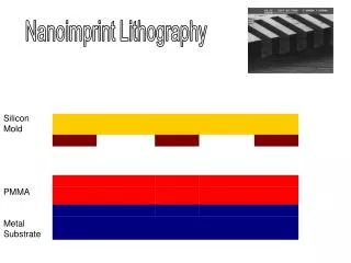
Imprinted etch barrier Residual layer Transfer layer Issue #2: NIL’s additional challenges • for Imprinting ultradense patterns • thickness of the imprinting resist, • residual layer • Metal Lift off • resist adhesion to the mold features
Silicon molds (SNAP technique) Self-aligned shadow mask deposition O2 Plasma Etch array of silicon posts 400um wide at 1.4mm spacing silicon nanowires with the best transfer results were selected (20um section out of 2-3mm array) NANO LETTERS 2006 Vol. 6, No. 3 351-354
metal patterns by NIL and subsequent lift-off process. • Schematic diagram of process flow: (a) application of mold to resist; (b) mold separation from the imprinted resist; (c) residual layer etching; (d) pattern transfer to the underlayer; (e) metal deposition; (f) metal lift-off. NANO LETTERS 2006 Vol. 6, No. 3 351-354
Image resist layer CONSIDERATIONS: • A high mechanical strength after curing, • low viscosity • good adhesion to and compatibility with the underlayer • a strong resistance to oxygen plasma dry-etching CHOSEN: UV-curable poly(dimethylsiloxane) material (Gelest, 87%), radical initiator (Irgacure 184, Ciba, 3%), and cross-linker (ethylene glycol dimethacrylate, Aldrich, 10%). Gentle reactive ion etching, The etch rate 0.3 nm/s TIP FOR SUCCESS: Thickness → Residual layer → Long etching step → Line edge roughness
Underlayer CONSIDERATIONS • adhere to glass substrate • firmly hold image resist layer during mold separation. • easily dissolved with solvents • serve as a planarizing layer. O2 plasma treatment The etch rates Underlayer: 1.3 nm/s , 22 times faster than Image layer: 0.06 nm/s. CHOSEN: LOL 1000 (Shipley Ltd.) TIP FOR SUCCESS: Thickness
SNAP-generated mold SEM images RESULTS AFM & SEM image 34 nm pitch metal cross-bar structure Image layer resist cell density of approximately 100 Gbit/cm2. cross-bar structure Metal Nanowires
CONCLUSIONS • SNAP to fabricate a mold for 17nm hp metal nanowires. • Bilayer resist structure was used for the nanoimprint lithography. • Nanowire patterns at 17 nm hp were successfully transferred to the underlayer by selective RIE without collapsing the resist patterns. • An array of 150 separated platinum nanowires was produced • A corresponding cross-bar structure was fabricated by repeating the imprinting process
The end • Questions?
RECIPE • On a borofloat glass substrate (Precision Glass & Optics, Santa Ana) • LOL layer was spin-coated and Baked in an oven at 90 °C for 30 min. • The thickness was modified with an oxygen plasma treatment to reach 25 nm. • 35 nm of the UV curable resist was spin-coated • Mold was treated with a releasing material in the vapor phase • Brought into contact with the UV-curable resist layer. • Substrate and mold pressed together in a vacuum. • Resist layer was cured for 15 min by UV irradiation through the glass substrate • Imprinting pressure of 80 psi in a purpose-built UV-based imprinting machine. • The mold was readily detached from the resist film with negligible separation force • Gentle reactive ion etching (CF4; 7 W at 2mTorr for 20 s; Cambridge, Inc., Plasmalab system 100) • to etch any residual layer under the trenches (Figure 2c). • The etch rate 0.3 nm/s for the image resist layer. • O2 plasma treatment (50 W at 20 mTorr for 25 s). • imprinted image patterns were then transferred to the LOL layer • The etch rate under O2 plasma was 1.3 nm/s for the LOL underlayer, 22 times faster than that of the image layer, 0.06 nm/s. With such a selective etching process, pattern transfer to the underlayer was accomplished without destroying the imprinted patterns on the image resist layer • Titanium (4 nm) and platinium (5 nm) were deposited by electron-beam evaporation (CHA, Fremont) at a deposition rate of 0.03 nm/s (Figure 2e). • Metal lift-off process was performed by • soaking the sample in a polymer remover (1165, Shipley Ltd.) at 110 C for 30 min • ultrasonic agitation for 1 min to produce the isolated metal nanowires at 17 nm hp
Additional slide REF[10] 1/3 • GaAs/Al0.8Ga0.2As on [100] GaAs substrate • BHF acid to etch AlGaAs layers • 20-30nm deep • Metal wires evaporated 36° w/r evaporative flux within vacuum chamber of e-beam evaporation system(deposited only on the GaAs layers) • Gold, chromium, aluminum, titanium, niobium, platinum, and nickel. • heat-curable epoxy film 10 nm thick, adhesion layer. The epoxy was cured at 150°C for 30 min, • sample was suspended upside down in KI (4 g)/I2 (1 g)/H2O (100 ml) to remove GaAs oxide layer at the nanowire-GaAs interface • The silicon wafer was removed, rinsed, and dried. • brief O2 plasma etch effectively removed the residual epoxy layer, if necessary SCIENCE 300 : 112 2003
Additional slide REF[10] 2/3 Pt nanowire arrays using the SNAP process (A) An electron micrograph of a 100-m section of an array of 60 nanowires. The bright line next to the nanowires is due to residual epoxy. (B) A higher resolution micrograph of same nanowires, showing 40 Pt wires 10 nm in diameter at a pitch of 60 nm, and 20 Pt wires 10nm in diameter at a pitch of 30 nm. (C) The highest density nanowire array fabricated, 20 Pt nanowires 8 nm in diameter at a pitch of 16 nm. (D) SEM image of SOI silicon nanowires. The 19 wires at the left are 18 nm wide at 30 nm pitch; the 40 wires at the right are 20 nm wide at 60 nm pitch. These wires were straight and continuous for >100um stretches SCIENCE 300 : 112 2003
Additional slide REF[10] 3/3 Fig. 4. A high-frequency nanomechanical resonator fabricated by the SNAP process. (A) The resonator contains nine Pt nanowires 20 nm in diameter suspended over a 0.75-m gap. (B) A resonance frequency (res) of 162.5 MHz is monitored as a function of increasing field strength, from 0 to 5 T. The 0-field measurement is subtracted from each of the readings. The response increases with field strength, with the 5-T recording presented as the darkest trace. (C) Electron micrograph of a few hundred Pt nanowire crossbar circuits fabricated by repeating the SNAP process. The crossbars are fabricated from Pt nanowires with pitches ranging from 20 to 80 nm. The central crossbar has a junction density of 5 1010 cm2, and the two crossbars to the lower left and right of this central one are at a junction density of 1011 cm2. Scale bars in (A) and (C), 500 nm. SCIENCE 300 : 112 2003