Download
1 / 14
190 likes | 578 Views
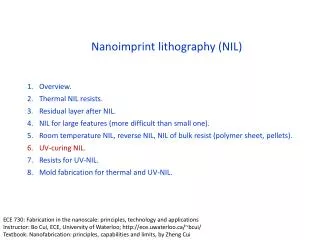
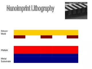
Yongshik Park EE235 04/14/08. Direct Nanoimprint Lithography. Nanoimprint Lithography (1994). Prof. Stephen Y. Chou. Imprint mold with 10nm diameter pillars. 10nm diameter holes imprinted in PMMA. 10nm diameter metal dots fabricated by NIL.

E N D
Yongshik Park EE235 04/14/08 Direct Nanoimprint Lithography
Nanoimprint Lithography (1994) Prof. Stephen Y. Chou Imprint mold with 10nm diameter pillars 10nm diameter holes imprinted in PMMA 10nm diameter metal dots fabricated by NIL NanoStructures Laboratory (Prof. Stephen Chou), http://www.princeton.edu/~chouweb/newproject/page3.html
Direct Nanoimprinting of Metal Nanoparticles Ko, S. H., et. al, Nano letters, Vol. 7, No. 7, p1869, 2007
SAM-encapsulated Nanoparticles • Smaller size of nanoparticle has lower melting temperature. • 2nm particle 140℃ • 140℃ofsintering makes low resistivity of material • From particles to bulk material Ko, S. H., et. al, Nano letters, Vol. 7, No. 7, p1869, 2007
Nanoimprinted gold structures • Minimum feature size is 0.45nm because PDMS mold’s poor resolution. (There is more room to be optimized) • There is few residual material because of low viscosity of solution Ko, S. H., et. al, Nano letters, Vol. 7, No. 7, p1869, 2007
Nanoscale patterning on flexible substrate Park, I., et. al, Advanced Materials, Vol. 20, p489, 2008
Electrical and structural characterization under Cyclic bending deformation Park, I., et. al, Advanced Materials, Vol. 20, p489, 2008
Electrochemical Nanopatterning • RbAg4I5 is a fast and selective Ag ion conducting electrolyte. • Ag ions are mobile ions which is transported to opposite electrode without bulk mass transport of RbAg4I5 layer. Lee, M., et. al, Applied Physics Letters, Vol. 85, No. 16, p3552, 2004
Electrochemical Nanoimprinting • The process for high-resolution metallic nanopatterns • Solid-state superionic stamping • Stamp: Superionic conductor with a mobile cation (Ag2S) • Silver ions are mobile in superionic conductor Hsu, K. H., et. al, Nano Letters, Vol. 7, No. 2, p446, 2007
Electrochemical activity • The current density decrease as a result of the depletion of sliver at the anode and stabilizes with a low but nonzero value • Total transferred charge is nearly equal w.r.t. currents. • The same current profile is observed for each repetition. • There is settling down period for a stable shapeC Hsu, K. H., et. al, Nano Letters, Vol. 7, No. 2, p446, 2007
High-resolution transfer of channels and lines • The smallest line width and spacing is 50nm. • The feature height is around 100nm for the thicker lines and reduces to 40nm for the last two lines of width 90nm and 60nm. Hsu, K. H., et. al, Nano Letters, Vol. 7, No. 2, p446, 2007
Etch depth and rate • For a constant applied bias, the etch rate remains nearly constant and is independent of the depth to which the stamp has already traveled, facilitating the etching depth control. Hsu, K. H., et. al, Nano Letters, Vol. 7, No. 2, p446, 2007
Conclusions • Nanoimprint lithography is major breakthrough in nanopatterning because it can produce sub-10nm feature size over a large area with a high throughput and a low cost. • Direct nanoimprinting of metal nanoparticles is successfully demonstrated to high-resolution patterning and low temperature process. • The solid-state superionic stamping process produces high-resolution nanostructures and represents a new, efficient, and cost-effective avenue for current processes.