Download
1 / 33
330 likes | 488 Views
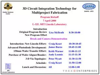
Introduction Original Program Review New Program Effort. Lisa McIlrath 8:30-10:00. Introduction: New Lincoln Effort:. Craig Keast 10:30-10:45. James Burns 10:45-11:00. Advanced Photodiode Development:. Keith Warner 11:00-11:15. 150mm Wafer Transfer Effort:. Andy Loomis 11:15-11:30.

E N D
Introduction Original Program Review New Program Effort Lisa McIlrath 8:30-10:00 Introduction: New Lincoln Effort: Craig Keast 10:30-10:45 James Burns 10:45-11:00 Advanced Photodiode Development: Keith Warner 11:00-11:15 150mm Wafer Transfer Effort: Andy Loomis 11:15-11:30 Purchase of Wafer Aligner/Bonder: 3-D Via Topologies: Peter Wyatt 11:30-11:50 Craig Keast 11:50-12:00 Schedule: Lunch and Discussion: All 12:00-1:00 3D Circuit Integration Technology for Multiproject Fabrication Program Kickoff 7 April 2000 L-325, MIT Lincoln Laboratory Break and Camera Demonstration
3D Circuit Integration Technology for Multiproject Fabrication TREX Enterprises: System Integration New Research in 3D Architectures and Systems Summary of Prior Results: Lisa McIlrath 8:40-9:00 Lisa McIlrath 9:00-9:30 New Program Overview: Steve Hawley 9:30-9:50 High Resolution Camera Design: Algorithms for Activity Detection with 3D Sensors: Victor Lum 9:50-10:05 Break and Camera Demonstration
N1 3D Photodiode Active Pixel • 10mm via • 32mm x 37mm • pixel area
3D Transfer/Via SEMs - 9/98 Deep and shallow 10mm vias - top view
6 mm via on 150mm wafer -- 7/23/99 Aluminum Oxide Adhesive
Photomicrograph of Imager Metal-1 Pad 3D Via
First 3D 64x64 Imager Results - 9/99 Dark Image Room Light Bright Light
Wafer-to-wafer bonding process under development at Lincoln Laboratory Traveller of NU 3D process delivered to Lincoln Complete devices from North 3 and 4 runs Transfer Keith Warner to Lincoln - (task completed) NU - LL 3D Technology Transfer
V (xmax/x) .t A A V < B ? xmax.t Iph V B t t CLK 1 0 0 1 0 0 1 0 1 3D Pixel Design: Free-Running Sampled Oscillator
3D & 2D Pixel Layouts MOSIS HP 0.5mm process 30mm x 30mm pixel 3D SOI-CMOS 0.8mm process 2-layer 45mm x 45mm pixel
48x48 64x64 Circuits / Systems Design Status Pixel-Parallel A/D Imager Design -- Tests / Design Revs Complete 40nW / pixel @ 3.3V, 0.1% Residual Fixed Pattern Noise
Circuits / Systems Design Status 3rd Layer Design Taped Out 11/1/99 • On-chip VCO with 216 (65536) bit range • On-chip pixel-parallel 1st stage low pass filtering • Programmable resolution / dynamic range
Circuits / Systems Design Systems Environment • Camera demo system modified for 256 x 256 imager compatibility and interface upgrade • Research in future smart sensor designs: • Video tracking demo (V. Lum, M-Eng thesis) • Video feedback control architectures (A. Aina, PhD thesis)
Testbed DemonstrationCamera System (Demo Setup in Office)
Activity Monitoring Current image Background model Detected objects Object Tracking Using Adaptive Background Mixture Models Courtesy Chris Stauffer & Eric Grimson MIT Artificial Intelligence Laboratory
Phase- frequency detector Pixel Oscillator Adaptive memory Voltage- Controlled Oscillator Charge Pump A-Data Store Analog Memory with Digital Feedback Change detector
Multimode memory module Pixel Input active F.D. Monitor enable VCO Charge Pump active F.D. Monitor enable VCO Charge Pump Problem: VCO tracks new values faster than monitor detects them
Compensated Memory Solution: Integrate a low pass filter into the loop active Pixel Input F.D. Filter enable VCO Charge Pump
Creating the Filter Edge Counter active reset enable Compare Logic Edge Counter reset Pixel Input F.D. Edge Counter reset VCO Charge Pump
Detecting Activity Activity is determined by the temporal distance between pairs of unmatched edges Second unmatched edge Pixel Bitstream VCO output Input frequency change
Mixed Material System Integration High Bandwidth m-Processors Exploiting Different Process Technologies Advanced Imaging Technologies Large Focal Planes The Enabling Technology • Better circuit / interconnect ratio • “Unrestricted” vertical interconnections between layers • Low digital system power: P=CV2f SOI CMOS 3D
Phase I: Infrastructure Development Phase II: Small Volume 3D Processing Center for Multi-Project Runs Phase III: High Volume Manufacturing Path to Industrialization Goals: • Industry-Standard State-of-the-Art SOI/CMOS Process • Automated Wafer Align / Bonding / Interconnect Patterning
Process Development 0.8mm SOI/CMOS 0.18, 0.25 mm FDSOI Reliable low temperature oxide bonding High aspect ratio Tungsten plug fill Systems Development High Definition Imager Platform 3D-compatible near-IR imaging technique 3D CAD tools packaging Phase I Plan (25 months)
0.25mm FDSOI Test Pixel 14mm x 14mm (or less)
Explore best method for III-V incorporation with automated 3D process technology Proposal accepted from C. Fonstad, MIT, for selective InGaAs in Si growth Initial photodiode array lots for investigation Imager design unchanged Compatible with basic platform systems demo High-Resolution Near-IR Imager
Develop minimal toolset for 3D cell layout, design rule checking, netlist extraction Interface with commonly available tools, e.g., Magic, L-Edit, Spice Platform independent Remove major obstacle for new users in Phase II Plan: Build on prior work developed on Cadence tools Negotiate distribution agreement with Si-valley software vendor(s). 3D CAD Tools
Interface 3D camera with SXGA (1024x1280) display Identify military users Human factors issues High Definition Imager Platform