Download
1 / 44
440 likes | 524 Views
Understanding the motivation for Clock Data Recovery (CDR) using Deserializer with insights from Prof. Michael Green. Learn about the significance of aligning data and clock signals, PLL synchronization, NRZ and RZ formats, phase detection, and DFF operation in CDR circuits. Explore the implications of non-idealities in phase detection for effective CDR implementation.

E N D
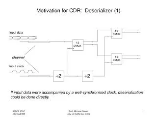
Motivation for CDR: Deserializer (1) Input data Input clock 1:2 DMUX 1:2 DMUX channel 1:2 DMUX If input data were accompanied by a well-synchronized clock, deserialization could be done directly. Prof. Michael Green Univ. of California, Irvine
Motivation for CDR (2) • Providing two high-speed channels (for data & clock) is expensive. • Alignment between data & clock signals can vary due to different channel characteristics for the different frequency components. Hence retiming would still be necessary. Clock Data retimed data Clock Recovery circuit input data recovered clock PLLs naturally provide synchronization between external and internal timing sources. A CDR is often implemented as a PLL loop with a special type of PD... Prof. Michael Green Univ. of California, Irvine
Return-to-Zero vs. Non-Return-to-Zero Formats NRZ f Tb RZ f 0 1 0 1 1 1 0 RZ spectrum has energy at 1/Tc conventional phase detector can be used. NRZ spectrum has null at 1/Tc ?? Prof. Michael Green Univ. of California, Irvine
Vdata Vd VRCK Phase Detection of RZ Signals Vdata VRCK Vd • Phase detection operates same as for clock signals for logic 1. • Vd exhibits 50% duty cycle for logic 0. • Kpd will be data dependent. Prof. Michael Green Univ. of California, Irvine
Vdata Vd VRCK Phase Detection of NRZ Signals Vdata VRCK Vd Since data rate is half the clock rate, multiplying phase detection is ineffective. • RZ signals can use same phase detector as clock signals • RZ data path circuitry requires bandwidth that is double that of NRZ. • Different type of phase detection required for NRZ signals. Prof. Michael Green Univ. of California, Irvine
Idea: Mix NRZ data with delayed version of itself instead of with the clock. Example: 1010 data pattern (differential signaling) Tb X X = = fundamental generated Prof. Michael Green Univ. of California, Irvine
QI QI D CK CK CK CK CK CK CK CK latch: CK Q D CK CK CK Slave Master Operation of D Flip-Flips (DFFs) DFF: CMOS transmission gate: Ideal waveforms: Symbol: D0 D1 D2 D D Q CK Q D0 D1 D2 No bubble Q changes following rising edge of CK Prof. Michael Green Univ. of California, Irvine
DFF Setup & Hold Time At CK rising edge, the master latches and the slave drives. D tsetup thold CK Q When a data transition occurs within the setup & hold region, metastability occurs. Prof. Michael Green Univ. of California, Irvine
QI CK CK CK CK D0 D1 D2 D CK Q D CK CK CK D1 D2 D0 Q CK Slave Master tck-q DFF Clock-to-Q Delay tck-q is determined by delays of tgate and inverter. Prof. Michael Green Univ. of California, Irvine
P Din Q RCK synchronized: RCK RCK early: D0 D3 D2 D1 D2 D3 D0 D1 D0 D2 D2 D3 D0 D1 D1 D3 Realization of Data/Data Mixing : Same as Din, synchronized with RCK Din RCK Q P D0 D1 D2 D3 D0 D1 D2 D3 D1 D2 D3 D4 D1 D2 D3 D4 Delay between Din to Q is related to phase between Din & RCK Prof. Michael Green Univ. of California, Irvine
RCK early ( < 0): Dt Tb Define zero phase difference as a data transition coinciding with RCK falling edge; i.e., RCK rising edge is in center of data eye. RCK synchronized ( = 0): Din RCK Q P Dt Tb Prof. Michael Green Univ. of California, Irvine
Phase detector characteristic also depends on transition density: P Din Q RCK 0011… pattern: 0101… pattern: Din RCK Q P In general, where average transition density Prof. Michael Green Univ. of California, Irvine
Constructing CDR PD Characteristic a = 1 a = 0.5 a = 0.25 -p +p Df slope: intercept: Both slope and offset of phase-voltage characteristic vary with transition density! Prof. Michael Green Univ. of California, Irvine
To cancel phase offset: P Din Q RCK R D2 D3 D1 D0 D3 D1 D0 D2 QR Q RCK QR R Always 50% duty cycle; average value is +1 = 1 Kpd still varies with , but offset variation cancelled. = 0.5 -p +p C. R. Hogge, “A self-correcting clock recovery circuit,” IEEE J. Lightwave Tech., vol. 3, pp. 1312-1314, Dec. 1985. -1 Prof. Michael Green Univ. of California, Irvine
Transconductance Block Iout+ Iout- P+ P- R- R+ ISS ISS Prof. Michael Green Univ. of California, Irvine
Due to inherent mixing operation, Hogge PD is not a good frequency detector. A frequency acquisition loop with a reference clock is usually needed: J. Cao et al., “OC-192 transmitter and receiver in 0.18m CMOS,” JSSC. vol. 37, pp. 1768-1780, Dec. 2002. Prof. Michael Green Univ. of California, Irvine
Non-Idealities in Hogge Phase Detector:A. Clock-to-Q Delay (1) Din P RCK Din Q RCK Q tck-Q R QR QR P tck-Q R Prof. Michael Green Univ. of California, Irvine
Non-Idealities in Hogge Phase Detector:A. Clock-to-Q Delay (2) Result is an input-referred phase offset: Din RCK +a tck-Q fos Q -a tck-Q QR P R Prof. Michael Green Univ. of California, Irvine
Non-Idealities in Hogge Phase Detector:A. Clock-to-Q Delay (3) tck-Q Din RCK Dout Phase offset moves RCK away from center of data, making retiming less robust. Din CDR RCK Prof. Michael Green Univ. of California, Irvine
Non-Idealities in Hogge Phase Detector:A. Clock-to-Q Delay (4) Use a compensating delay: Din Set DDt Dt Dt P RCK Din Q Q RCK tck-Q QR R P QR R tck-Q Prof. Michael Green Univ. of California, Irvine
P Din Q Din RCK RCK R Q QR QR P R P and R are offset by 1/2 clock period Non-Idealities in Hogge Phase Detector:B. Delay Between P & R (1) Prof. Michael Green Univ. of California, Irvine
Non-Idealities in Hogge Phase Detector:B. Delay Between P & R (2) P R Average value of Vcontrol is well-controlled, but resulting ripple causes high-frequency jitter. P Vcontrol Din Q RCK to VCO R QR Prof. Michael Green Univ. of California, Irvine
Non-Idealities in Hogge Phase Detector:B. Delay Between P & R (3) Idea: Based on R output, create compensating pulses: Standard Hogge/charge pump operation for single input pulse: Din RCK DFF Din RCK latch Q QR P (up) latch R (dn) Vcontrol latch Prof. Michael Green Univ. of California, Irvine
Non-Idealities in Hogge Phase Detector:B. Delay Between P & R (4) Cancels out effect of next pulse Din Din RCK Q1 RCK Q1 DFF Q2 Q3 Q2 latch Q4 P (up) Q3 R (dn) latch P’(dn) R’(up) Q4 latch Vcontrol Prof. Michael Green Univ. of California, Irvine
60 40 20 response from ideal linear PD PD Differential Output (mV) 0 -20 -40 -60 simulated result of one linear PD -50p -40p -30p -20p -10p 0 10p 20p 30p 40p 50p Data Delay in regard to Clock (s) Other Nonidealities of Hogge PD (1) Prof. Michael Green Univ. of California, Irvine
Other Nonidealities of Hogge PD (2) Effect of Transition Density: Prof. Michael Green Univ. of California, Irvine
Other Nonidealities of Hogge PD (3) Effect of DFF bandwidth limitation: Prof. Michael Green Univ. of California, Irvine
Other Nonidealities of Hogge PD (4) Effect of XOR bandwidth limitation: Since the PD output signals are averaged, XOR bandwidth limitation has negligible effect. Prof. Michael Green Univ. of California, Irvine
Other Nonidealities of Hogge PD (5) Effect of XOR Asymmetry: Prof. Michael Green Univ. of California, Irvine
Binary Phase Detectors Idea: Directly observe phase alignment between clock & data Clock falling edge late: Increase Vcontrol Clock falling edge centered: No change to Vcontrol Clock falling edge early: Decrease Vcontrol Ideal binary phase-voltage characteristic: Also known as “bang-bang” phase detector +1 -1 Prof. Michael Green Univ. of California, Irvine
D Flip-Flop as Phase Detector Din Early clock: Data transitions align with clock low RCK Din Late clock: Data transitions align with clock high RCK Top (bottom) DFF detects on Din rising (falling) edge; DFF selected by opposite Din edge to avoid false transitions due to clock-q delay. Realization using double-clocked DFF; note that RCK/Din connections are reversed: VP RCK = RCK VP Prof. Michael Green Univ. of California, Irvine
tsetup thold D CK Q What happens if Df=0? • If transition at D input occurs within setup/hold time, metastable operation results. • Q output can “hang’’ for an arbitrarily long time if zero crossings of D & CK occur sufficiently close together. • Metastable operation is normally avoided in digital circuit operation(!) Prof. Michael Green Univ. of California, Irvine
Dog Dish Analogy ? ? ? A dog placed equidistant between two dog dishes will starve (in theory). Prof. Michael Green Univ. of California, Irvine
Non-Idealities in Binary DFF Phase Detector Metastable operation difficult to characterize & simulate, varies widely over processing/temperature variations. Kpd (and therefore jitter transfer function parameters) are difficult to analyze. Exact value of Kpd depends on metastable behavior and varies with input jitter. Large-amplitude pattern-dependent variation is present in phase detector output while locked. During long runs phase detector output remains latched, resulting in VCO frequency changing continuously: RCK VP Prof. Michael Green Univ. of California, Irvine
Idea: Change VCO frequency for only one clock period RCK VP RCK early RCK late Circuit realization should sample data with clock (instead of clock with data) while maintaining bang-bang operation. Prof. Michael Green Univ. of California, Irvine
DN Alexander Phase Detector UP Q2 Q1 Q3 Q4 RCK RCK Q1 Q2 Q3 Q4 DN UP RCK early Q1 leadsQ3;Q2/Q4 in phase RCK late Q3 leadsQ1;Q1/Q4 in phase Prof. Michael Green Univ. of California, Irvine
Simulation Results: Alexander PD DFF outputs VCO control voltage Prof. Michael Green Univ. of California, Irvine
Simulation Comparison: Linear vs. Binary Vcontrol Vcontrol Binary PD Linear PD • very small freq. acquisition range • low steady-state jitter • high freq. acquisition range • high steady-state jitter Prof. Michael Green Univ. of California, Irvine
Half-Rate CDRs To relax speed requirements for a given fabrication technology, a half-rate clock signal can be recovered: input data Din RCK full-rate recovered clock RCK2 half-rate recovered clock • Can be used in in applications (e.g., deserializer) where full-rate clock is not required. • Duty-cycle distortion will degrade bit-error ratio & jitter tolerance compared to full-rate versions. Prof. Michael Green Univ. of California, Irvine
Din DA RCK2 DB Idea 1: Input data can be immediately demultiplexed with half-rate clock RCK2 Din D0 D1 D2 D3 D4 DA D2 D4 D0 synchronized with clock transitions DB D3 D1 Prof. Michael Green Univ. of California, Irvine
Din XA DA Splitting D flip-flops into individual latches: RCK2 latch latch XB DB latch latch RCK2 Din XA synchronized with both RCK2 & Din XB DA synchronized with RCK2 These pulse widths contain phase information. DB Prof. Michael Green Univ. of California, Irvine
Complete Linear Half-Rate PD RCK2 XA DA Din Din RCK2 P R XA XB DB XB DA J. Savoj & B. Razavi, “A 10Gb/s CMOS clock and data recovery circuit with a half-rate linear phase detector,” JSSC, vol. 36, pp. 761-768, May 2001. DB Prof. Michael Green Univ. of California, Irvine
Idea 2: Observe timing between Din, RCK and quadrature RCKQ Din Din RCK RCK RCKQ RCKQ S0 S1 S2 S0 S1 S2 Clock early Clock late Phase logic: S0, S2 sampled with RCK transitions S1 sampled with RCKQ transitions clock early clock late no transition Prof. Michael Green Univ. of California, Irvine
DI Din VPD RCK DQ J. Savoj & B. Razavi, “A 10-Gb/s CMOS clock and data recovery circuit with a half-rate binary phase detector,” JSSC, vol. 38, pp. 13-21, Jan. 2003. RCKQ Din Din RCK RCK RCKQ RCKQ DI DI DQ DQ VPD VPD Clock early Clock late Prof. Michael Green Univ. of California, Irvine