Download
1 / 21
220 likes | 248 Views
Explore Si micromachining techniques including Bulk and Surface approaches. Understand key etching and lithography steps, isotropic vs. anisotropic etching, and applications in mechanical testing and Cantilever Si Beams fabrication. Learn about Dry-Etching Based Bulk Micromachining.

E N D
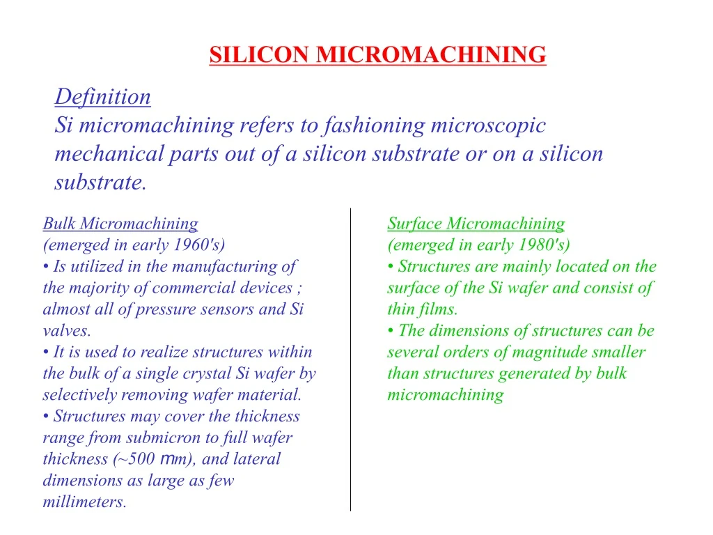
SILICON MICROMACHINING Definition Si micromachining refers to fashioning microscopic mechanical parts out of a silicon substrate or on a silicon substrate. • Bulk Micromachining • (emerged in early 1960's) • Is utilized in the manufacturing of the majority of commercial devices ; almost all of pressure sensors and Si valves. • It is used to realize structures within the bulk of a single crystal Si wafer by selectively removing wafer material. • Structures may cover the thickness range from submicron to full wafer thickness (~500 mm), and lateral dimensions as large as few millimeters. • Surface Micromachining • (emerged in early 1980's) • Structures are mainly located on the surface of the Si wafer and consist of thin films. • The dimensions of structures can be several orders of magnitude smaller than structures generated by bulk micromachining
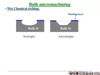
SILICON BULK MICROMACHINING • Lithography and etching are the key technological steps for bulk micromachining. • Basic Etch Steps : • (i) Wet isotropic etching. • (ii) Wet anisotropic etching. • (iii) Plasma isotropic etching. • (iv) Reactive ion etching (RIE). • (v) Etchstop techniques.
Isotropic and Anisotropic Wet Etching • In diamond and zinc-blend lattices, the (111)-plane is more closely packed than the (100)-plane and, hence, for any given etchant the etch rate is expected to be slower for the (111) plane. • For most wet etchants this difference in etch rates with orientation is insignificant : the result is that with most wet etchants etching is isotropic. • However, some wet etchants have the property of dissolving a given crystal plane of a semiconductor much faster than other planes ; i. e., these etchants have etch rates that are orientation dependent.
Anisotropic Etching Characteristics of Crystalline Si • The width of the bottom surface, W, is Wo is the width of the window on the wafer surface an h is the etched depth.
Example (1) : Mechanical Velcro (I) Objective : To apply isotropic and anisotropic wet etching to fabricate dense regular arrays of microstructures which act as surface adhesives. Han etal., JMEMS 1(1), 37 (1992)
(II) Process Flow The caps are 1.0 mm of SiO2 atop Si pedestals.
(III) Mechanical Testing : Method • Patterned samples, nominally 8 mm x 8 mm were interlocked by applying a load to the upper substrate ; the insertion pressure was monitored by placing the entire assembly on an electronic force scale. • The bond strength of the mating structures was characterized by direct measurements of the tensile load needed to induce failure : bond strength is determined by applying a tensile load through a pulley and measuring the force necessary for separation. • Separation of the samples (failure) is always accompanied by damaged areas on corresponding regions of the mating surfaces : this is interpreted as the samples interlocking only over damaged regions. • The fraction of damaged area was found to be proportional to the initial loading (insertion pressure).
(IV) Analysis • Assuming simple cantilever : • The bending stress, s, is • y is the distance from the neutral surface. b and h are the width and thickness of the rectangular cross-section. • For x = 0 and y = ± h/2 Pn is the interaction force between the tabs and l is the length of the tab.
The maximum shearing stress is at the neutral surface (y = 0) : The ratio of the two stresses is Measurements indicate that failure occurs when From the figure : Using : We get : Substituting design values :
Example (2) : Undoped Cantilever Si Beams (I) Objective : To fabricate cantilever beams oriented in the (100) direction on (100) silicon wafers. Choi and Smits ; JMEMS, 2(2), 82 (1993)
(II) Flow Process : Masks To construct a Si cantilever beam of width Wb, thickness tb, and length lb. For mask 1 (etching in NaOH) : To free the Si cantilever in the second NaOH etching, we need for mask 2 : W1 = 190 mm, W2 = 110 mm, d = 300 mm, and l1 =l2 = {450, 680, 900, 1360, 1810} mm.
Dry-Etching Based Bulk Micromachining • The type, shape and size of single-crystal silicon (SCS) structures that can be fabricated using anisotropic wet chemical etch techniques are severely limited. • Dry-etch based processes have been developed. • The most important of these processes is a process called SCREAM for single crystal reactive etching and metallization process. • SCREAM uses RIE processes to fabricate released SCS structures with lateral feature sizes down to 250 nm and with arbitrary structure orientations on a Si wafer. • SCREAM includes process options to make integrated, side-drive capacitor actuators. • A compatible high step-coverage metallization process using metal sputter deposition and isotropic metal dry etch is used to form side-drive electrodes. This metallization process complements the Si RIE processes used to form the movable SCS structures.
Example (3) : Straight Cantilever Beam with Integrated Al Electrodes (I) Objective : To fabricate a free-standing cantilever beam 200 mm long, 0.8 mm wide, and 3.5 mm thick coated with a 150 nm thick silicon dioxide layer. Zhang and MacDonald, JMM, pp. 31-38 (1992).