Combinational Logic
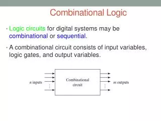
Combinational Logic. Changes in input values are reflected immediately (subject to the speed of light and electrical delays) on the outputs Each gate has an associated “electrical delay” Delays are often ignored for the purpose of the logic design (but not for the real implementation!)

Combinational Logic
E N D
Presentation Transcript
Combinational Logic • Changes in input values are reflected immediately (subject to the speed of light and electrical delays) on the outputs • Each gate has an associated “electrical delay” • Delays are often ignored for the purpose of the logic design (but not for the real implementation!) • As soon as inputs change, the outputs change – no memory of what happened before • (at least conceptually)
Call button Blue light Bit Storage Cancel button Blue light Call button Bit Storage Cancel button Q Call 2. Call button released – light stays on Cancel Call button Blue light Bit Storage Doesn’t work. Q=1 when Call=1, but doesn’t stay 1 when Call returns to 0 Cancel button Need some form of “feedback” in the circuit 3. Cancel button pressed – light turns off Example Needing Bit Storage • Flight attendant call button • Press call: light turns on • Stays on after button released • Press cancel: light turns off • Logic gate circuit to implement this? 1. Call button pressed – light turns on a a
S 1 S 1 S 0 S 1 Q Q Q 1 1 1 Q 0 0 1 1 0 t t t t 1 S 0 1 t 0 1 Q 0 First attempt at Bit Storage • We need some sort of feedback • Does circuit on the right do what we want? • No: Once Q becomes 1 (when S=1), Q stays 1 forever – no value of S can bring Q back to 0 Q S t
Reset Set Q Basic NOR (SR) Latch • When Set = 0, Reset = 1 Q = 0 • When Set = 1, Reset = 0 Q = 1 • When Set = Reset = 0 Q = memory • When Set = Reset = 1 Q = 0
R Q Q S Basic NOR Latch Redrawn memory state
R Q Q S t t t t t t t t t t 1 2 3 4 5 6 7 8 9 10 1 R 0 1 S 0 1 Q ? 0 1 Q ? 0 Timing Analysis of Basic Latch • What happens at t10?? • S and R both go from 1 to 0 simultaneously • If gate delays are exactly the same oscillation!!!
R Q Clk Q S Gated SR Latch • To get better control of the state changes, we must limit when the input signals affect the outputs • Outputs change only when Clk = 1 • Clk acts as an Enable signal undefined since we don't know which stable state will result
S Q Clk Q R Q S Clk R Q Comments on Latches • Need to avoid the unstable state • Note that all other states have “correct” Q and Q • Can use the cross-coupled NOR approach, or can use the cross-coupled NAND approach • All gates are the same type
Q D Clk Q Gated D Latch • Provide only a single control signal D (for Data) • More common than SR latch, and simpler S D (Data) Q Clk Q R
t t t t 1 2 3 4 Clk D Q Time D Latch Timing Diagram • Output Q changes only when Clk = 1 • Q tracks D when Clk = 1 • This latch is level-sensitive since the output is sensitive to the level of the clock
Q D Q Master Slave Q Q D D Q D Q Clk Clk Clock Q Q Q Master-Slave D Flip-Flop • Desire to remove the level-sensitive nature • Want changes in Q only on the transition of the Clk signal from 1 0 (or from 0 1) • When Clock = 1, master D latch tracks D; slave D latch remains unchanged (Q remains fixed) • When Clock = 0, master D latch is unchanged; slave D latch tracks Qm negative edge-triggered flip-flop
Clock D Q m Q = Q s Master Slave Q Q m s Q Q D D Q D Clk Clk Clock Q Q Q Timing of Master-Slave D Flip-Flop • Changes to Q occur only on the negative edge of the Clock
Terms, Reviewed • Latch • Two NANDs (or NORs) used to store one bit • Gated latch • Latch with an control enable, called Clk • Two basic types: SR and D, both level sensitive • Master-slave flip-flop • State changes only on clock edge; made from two gated D latches
Registers • A flip-flop stores one bit of information • When you want to store n bits register • n flip-flops used • Clock is shared by all so action is synchronous with clock edge • Some common register types • Simple register • Shift register • Parallel access shift register • Lots of counters: up counter, down counter, BCD counter, ring counter, Johnson counter
Parallel output Q Q Q Q 3 2 1 0 Q Q Q Q D D D D Q Q Q Q Parallel input Clock Simple 4-bit Register • A standard 4 bit register using D flip flops
Parallel output Q Q Q Q 3 2 1 0 Q Q Q Q D D D D Q Q Q Q Parallel input Load Clock 4-bit Register with Load Control • Controlling the load capability

