COMBINATIONAL LOGIC ANALYSIS
Learn the definition, types, and applications of combinational logic circuits. Discover how to implement logic circuits from Boolean expressions and truth tables. Explore the concept of universal gates. Practice analyzing circuits with input and output waveforms.

COMBINATIONAL LOGIC ANALYSIS
E N D
Presentation Transcript
Chapter 5 COMBINATIONAL LOGIC ANALYSIS
Combination of basic gates to form circuits that can carry out a desired application. • In combinational logic, the output level is at all times dependent on the combination of input levels • Combinational logic circuits contain no memory (no ability to store information) DEFINITION OF COMBINATIONAL LOGIC
AND-OR LOGIC • Represents SOP implementation – AND gate for product term, OR gate for summing the product terms
AND-OR-INVERT LOGIC • Represents POS implementation – AND gate for product term, OR gate for summing the product terms, NOT gate to complement the AND-OR circuit
XOR LOGIC • Combination of 2 AND gates, 1 OR gate, & 2 NOT gates. • Considered a type of logic with own unique symbol ( ).
XNOR LOGIC • The complement of XOR logic.
Implement logic circuit fromBoolean Expression • Example: Logic circuit for X = AB + CDE
Draw logic circuit for X = AB(CD + EF) Exercise 1
Implement logic circuit fromTruth-table • First, write the SOP expression from the Truth Table. Then, implement the logic circuit.
NAND gate is a universal gate because it can be used to produce the NOT, AND, OR and NOR functions. Universal Gate
NOR gate is also a universal gate because it can be used to produce the NOT, AND, OR and NAND functions. Universal Gate
NAND NEGATIVE OR
NOR NEGATIVE AND
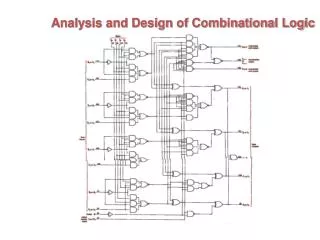
The output of a logic circuit at any given time depends on the input at that particular time. • Example: Determine the final output waveform X for the circuit in figure below, with input waveforms A,B and C as shown.